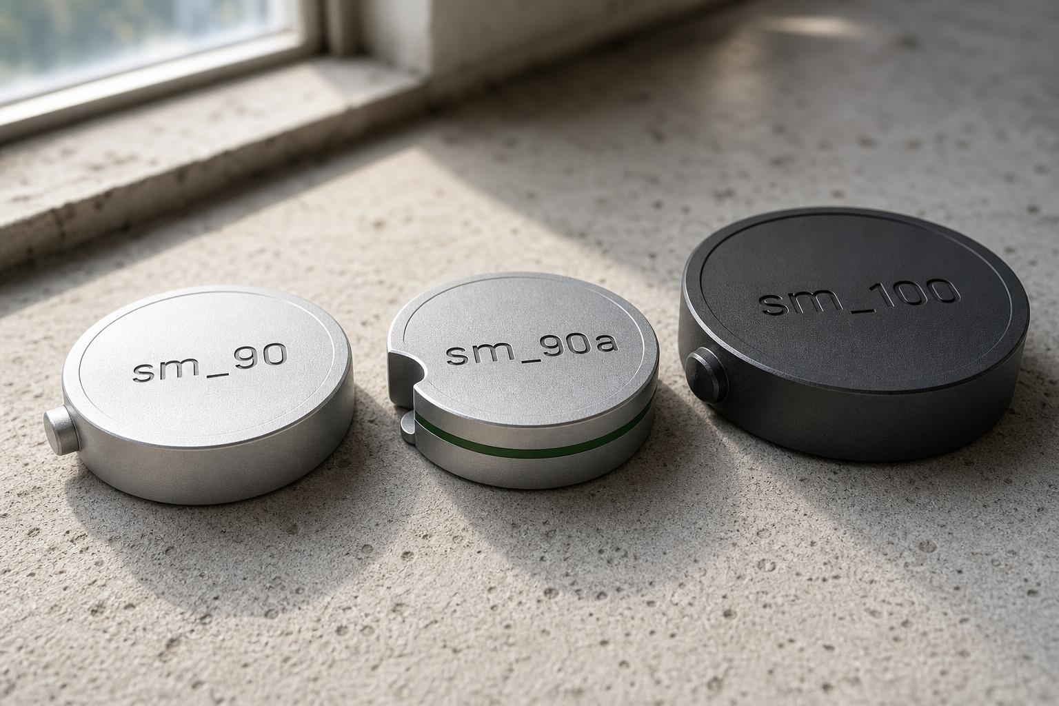
GPUSmith Article
CUDA Compute Capability by GPU: The Complete sm_75-sm_121 Chart
Inside this article
- 01Executive Summary
- 02Introduction and Background
- 03The Compute Capability Numbering System: What sm_XX Actually Means
- 04The Complete CUDA Compute Capability Table: Turing Through Blackwell
- 05Architecture by Architecture: From sm_75 to sm_121
- 06Analysis of Key Segments: Data Center, Workstation, Consumer, and Embedded GPUs
- 07Data Analysis and Evidence
- 08Case Studies and Real-World Examples
- 09Implications and Future Directions
- 10Frequently Asked Questions (FAQs)
- 11Conclusion
Here is the content with internal links added:
Executive Summary
CUDA compute capability is the version number, written as a major and minor pair such as 8.9 or 9.0, that NVIDIA assigns to every CUDA-capable GPU to indicate which hardware features and instructions that GPU supports [1]. As of July 2026, the officially supported range spans compute capability 7.5 (Turing, streaming multiprocessor version sm_75) through 12.1 (Blackwell, sm_121), with compute capability 9.0 (Hopper, sm_90) and 10.0/10.3 (Blackwell and Blackwell Ultra, sm_100/sm_103) anchoring most current data-center AI deployments [2]. This report compiles the complete, current mapping from GPU model to compute capability, explains the sm_XX naming convention, and answers the practical questions developers ask when setting build flags for PyTorch, TensorFlow, and CUTLASS.
The GPU-to-compute-capability lookup breaks down by architecture as follows: Turing GPUs (Tesla T4, GeForce RTX 20-series, Quadro RTX) sit at compute capability 7.5; Ampere data-center parts (A100, A30) sit at 8.0 while Ampere consumer and professional cards (RTX 3050 through RTX 3090 Ti, RTX A2000 through A6000) sit at 8.6, and Jetson AGX Orin uses 8.7 [2]; Ada Lovelace (L4, L40, L40S, GeForce RTX 40-series) sits at 8.9; Hopper (H100, H200, GH200) sits at 9.0; Blackwell data-center GPUs (B100, B200, GB200) sit at 10.0, Blackwell Ultra (B300, GB300) sits at 10.3, Jetson Thor sits at 11.0, and consumer/workstation Blackwell (GeForce RTX 50-series, RTX PRO Blackwell) sits at 12.0, with the GB10-based DGX Spark at 12.1 [2]. NVIDIA's CUDA Toolkit and Architecture Matrix confirms that Turing (7.5) support began with CUDA 10.0 and remains ongoing, while Hopper (9.0) support began with CUDA 11.8 and Blackwell (10.0/12.0) support began with CUDA 12.8 [3].
A critical and frequently misunderstood distinction is that compute capability 8.9 (Ada) and 9.0 (Hopper) are not simply sequential steps: Hopper introduced FP8 Tensor Core support, distributed shared memory, thread block clusters, and the Tensor Memory Accelerator, none of which exist on 8.x devices, and beginning at 9.0 NVIDIA introduced "architecture-specific" compiler targets (the "a" suffix, such as compute_90a) whose code cannot run on any other compute capability [4]. NVIDIA's own CUTLASS library confirms that using the plain sm_90 target instead of sm_90a for a kernel that relies on Hopper-specific Tensor Core instructions is expected to fail with a runtime error [5]. Similarly, sm_90 and sm_100 are separate, non-interchangeable targets, and within Blackwell itself sm_100 (data-center) and sm_120 (consumer) are two distinct, mutually incompatible families despite sharing the "Blackwell" marketing name (Source: arnon.dk). For developers configuring frameworks, TensorFlow's official pip wheels support "CUDA architectures 3.5, 5.0, 6.0, 7.0, 7.5, 8.0 and higher" [6], while PyTorch is built via the TORCH_CUDA_ARCH_LIST environment variable, which for full Blackwell coverage should be set to include values through "12.1+PTX" (Source: arnon.dk).
The stakes of getting this right are compounding: NVIDIA's data-center and AI segment revenue has grown roughly 1,300-fold over twelve years, from $57 million to more than $75 billion per quarter [7], and independent estimates place NVIDIA's share of the AI accelerator market at roughly 80 to 90% by revenue, though the exact figure varies by source and methodology [7] [8] [9]. Real-world deployments illustrate the range: Europe's first exascale supercomputer, JUPITER, runs roughly 24,000 NVIDIA GH200 (compute capability 9.0) superchips [10], while AWS EC2 P5, Microsoft Azure ND H100 v5, and Google Cloud A3 all standardize on eight H100 GPUs (also compute capability 9.0) per node [11] [12] [13], and CUDA Toolkit 13.0 formally dropped support for every GPU below compute capability 7.5, removing Maxwell, Pascal, and Volta from active toolchains [14]. This report walks through the full compute-capability table, the naming and compiler-target system behind it, the segment-by-segment breakdown across data center, workstation, consumer, and Jetson hardware, and the practical implications for anyone selecting GPUs or setting compiler flags in mid-2026.
Introduction and Background
Every NVIDIA GPU that supports CUDA (Compute Unified Device Architecture) carries a version number called its compute capability, expressed as a major and minor pair such as 7.5, 8.9, or 10.0 [1]. This number is not a marketing label and it is not the same as a GeForce, Quadro, or Tesla product name; it is a hardware capability version that determines which CUDA language features, Tensor Core data types, memory operations, and instruction sets a given GPU's streaming multiprocessors (SMs) physically support. CUDA (Compute Unified Device Architecture) is NVIDIA's proprietary parallel computing platform and programming model, created in 2004 and officially released in 2007, that lets developers use NVIDIA GPUs for general-purpose computation beyond graphics rendering [15]. Because compute capability governs what a compiled GPU kernel can actually execute, it is the single most important number for anyone building, deploying, or debugging GPU-accelerated software, whether that means training a large language model on a cluster of H100 GPUs or running local inference on a laptop RTX card.This report exists because the compute-capability landscape has become considerably more complex since NVIDIA's Hopper and Blackwell generations introduced architecture-specific and family-specific compiler targets that did not exist in earlier CUDA generations. A developer who learned CUDA on Pascal or Turing hardware, where compute capability 6.1 or 7.5 was a single, self-contained target, now has to navigate sm_90 versus sm_90a, sm_100 versus sm_100f versus sm_100a, and the fact that sm_120 (consumer Blackwell) is not binary-compatible with sm_100 (data-center Blackwell) despite both belonging to the same "Blackwell" marketing generation (Source: arnon.dk). Meanwhile, the practical question "what compute capability is my GPU" remains one of the most frequently searched CUDA queries, because the answer determines whether a given PyTorch or TensorFlow build will even recognize the installed hardware.
The scope of this report covers the full currently supported range, from compute capability 7.5 (Turing) through 12.1 (Blackwell's GB10 variant), the legacy range back to compute capability 1.0 for historical context, the exact GPU models NVIDIA associates with each compute capability as of July 2026, the CUDA Toolkit and driver support windows for each architecture, and the practical build-flag guidance developers need for PyTorch, TensorFlow, CUTLASS, and TensorRT. Two lookup methods are authoritative: NVIDIA's own CUDA GPU Compute Capability page, which "provides a comprehensive mapping from NVIDIA GPU models to their compute capability" [4], and the nvidia-smi command-line tool, which can be queried directly with nvidia-smi --query-gpu=name,compute_cap to report the installed GPU's name and compute capability at runtime [4].
The Compute Capability Numbering System: What sm_XX Actually Means
Compute capability numbers are written as X.Y, where X is the major version and Y is the minor version; for example, compute capability 12.0 has a major version of 12 and a minor version of 0 [1]. This number corresponds directly to a GPU's streaming multiprocessor (SM) version, so a GPU of compute capability 12.0 has SMs at version sm_120, and in the CUDA compiler toolchain the two notations are used interchangeably: NVIDIA's own documentation and the LLVM code NVIDIA has contributed both write compute capability X.Y as SMXY or sm_XY, for example 10.3 as SM103 or sm_103 [15]. Historically, one compute capability corresponded to one compiler target with no further qualification. That changed starting with Hopper.
Beginning with compute capability 9.0, NVIDIA introduced architecture-specific features: specialized capabilities such as Tensor Core operations that are not guaranteed to persist unmodified into later architectures and that require a dedicated compiler target using an a suffix, for example compute_90a or compute_100a [4]. Code compiled with an architecture-specific target can only run on the exact compute capability it was compiled for, with no forward or backward compatibility [4]. This is not a theoretical distinction: NVIDIA's own open-source CUTLASS library documents that several Hopper and Blackwell PTX instructions fall under this category of architecture-accelerated features, and thus require a sm_90a or sm100a target architecture, and that users are required to build CUTLASS with 90a as the target architecture to maximize performance on Hopper GH100, since building with the plain sm_90 target instead will cause a kernel using SM90a features to fail at runtime [5].
Starting with compute capability 10.0, NVIDIA layered in a second qualifier: family-specific features, selected with an f suffix such as compute_100f, introduced because some architecture-specific features turned out to be shared across more than one compute capability within the same silicon family [4]. As of mid-2026 there are two distinct Blackwell families: the 10.x family, covered by compute_100f and spanning sm_100 (B100/B200) and sm_103 (B300), and the 12.x family, covered by compute_120f and spanning sm_120 (RTX 50-series) and sm_121 (GB10/DGX Spark) (Source: arnon.dk). Critically, these two Blackwell families are not cross-compatible: sm_100f code does NOT run on sm_120 devices and vice versa (Source: arnon.dk). This is the practical answer to why "Blackwell" alone is not a sufficient specification when compiling CUDA code: the data-center GB100/GB200/GB300 silicon (sm_100/sm_103) and the consumer/workstation GB20x silicon (sm_120/sm_121) are separate compilation targets that happen to share a marketing generation name. NVIDIA's own compute-capabilities documentation illustrates the same 10.0/10.3 family relationship directly: the compute_100f target is compatible with devices of Compute Capability 10.0 and Compute Capability 10.3 [4]. CUTLASS itself is expected to be efficient on Volta, Turing, Ampere, Ada, and Hopper architecture based NVIDIA GPUs, and separately documents CuTe DSL support extending to Ampere, Hopper, and Blackwell Tensor Cores, illustrating how even NVIDIA's own libraries track compute capability boundaries rather than marketing generation names [5].
Three feature-set tiers therefore coexist for every modern GPU:
- Baseline feature set: the plain compute capability target, such as
compute_100, with no suffix, offering the widest forward compatibility across the major version. - Family-specific feature set (the "f" suffix, from compute capability 10.0 onward): compatible with all devices sharing the same family, such as both sm_100 and sm_103 devices under
compute_100f. - Architecture-specific feature set (the "a" suffix, from compute capability 9.0 onward): the fullest available feature set, but locked to a single exact compute capability with zero portability.
For most developers targeting a fixed, known GPU fleet, the plain or family-specific target is the practical default; the architecture-specific "a" target is reserved for libraries like CUTLASS or custom kernels that need the absolute maximum performance from one specific chip and can accept the loss of portability.
The Complete CUDA Compute Capability Table: Turing Through Blackwell
NVIDIA maintains an official, continuously updated table mapping every currently supported GPU model to its compute capability at the CUDA GPU Compute Capability page, organized by data center, workstation/consumer, and Jetson product lines [2]. Table 1 below reproduces the currently supported range, compute capability 7.5 through 12.1, as published on that page and cross-checked against NVIDIA's CUDA Toolkit and Architecture Matrix and Wikipedia's community-maintained CUDA compute capability tables.
Table 1: CUDA Compute Capability by GPU, Turing (sm_75) Through Blackwell (sm_121)
| Compute Capability | SM / Compiler Target | Microarchitecture | Representative Data Center GPUs | Representative Workstation/Consumer GPUs | Representative Jetson/Embedded |
|---|---|---|---|---|---|
| 7.5 | sm_75 | Turing | NVIDIA T4 | GeForce RTX 2060 to RTX 2080 Ti, TITAN RTX, Quadro RTX 4000 to 8000, GTX 1650 Ti | (Jetson Xavier NX/AGX Xavier are compute capability 7.2, legacy) |
| 8.0 | sm_80 | Ampere (GA100) | A100, A30 | (none) | (none) |
| 8.6 | sm_86 | Ampere (GA10x) | A40, A10, A16, A2 | RTX A2000 to A6000, GeForce RTX 3050 to RTX 3090 Ti | (none) |
| 8.7 | sm_87 | Ampere (Orin) | (none) | (none) | Jetson AGX Orin, Orin NX, Orin Nano |
| 8.9 | sm_89 | Ada Lovelace | L4, L40, L40S | RTX 2000 Ada to RTX 6000 Ada, GeForce RTX 4050 to RTX 4090 | (none) |
| 9.0 | sm_90 / sm_90a | Hopper | H100, H200, GH200 | (none) | (none) |
| 10.0 | sm_100 / sm_100a / sm_100f | Blackwell | B100, B200, GB200 | (none) | (none) |
| 10.3 | sm_103 / sm_103a / sm_103f | Blackwell Ultra | B300, GB300 | GB300 (DGX Station) | (none) |
| 11.0 | sm_110 / sm_110a (was sm_101 pre-CUDA 13) | Blackwell (Thor) | (none) | (none) | Jetson T5000, Jetson T4000 |
| 12.0 | sm_120 / sm_120a / sm_120f | Blackwell (consumer) | RTX PRO 6000/4500 Blackwell Server Edition | RTX PRO 6000/5000/4500/4000/2000 Blackwell, GeForce RTX 5050 to RTX 5090 | (none) |
| 12.1 | sm_121 / sm_121a | Blackwell (GB10) | (none) | NVIDIA GB10 (DGX Spark) | (none) |
Sources: developer.nvidia.com/cuda/gpus [2]; docs.nvidia.com CUDA Programming Guide [4]; arnon.dk architecture reference (Source: arnon.dk) as of July 2026.
Reading this table left to right, three patterns stand out. First, data center and consumer product lines frequently share a major compute capability version but diverge on minor version: Ampere data center parts sit at 8.0 while Ampere consumer and professional cards sit at 8.6, reflecting a different balance of FP64 throughput, memory subsystem, and SM count even though both are "Ampere." Second, embedded Jetson hardware routinely trails its data-center counterpart in numbering scheme even when architecturally related, as with Jetson AGX Orin at 8.7 while data-center Ampere spans 8.0 and 8.6, and Jetson Thor landing at 11.0 despite following the 10.x Blackwell data-center generation. Third, and most consequential for compiler-flag decisions, the newest generation subdivides further than any prior one: Blackwell alone spans five distinct compute capabilities (10.0, 10.3, 11.0, 12.0, 12.1) across four different product families, a degree of fragmentation with no precedent in Kepler, Maxwell, Pascal, Turing, or Ampere.
For anyone asking "what compute capability is my GPU," the fastest reliable answer, short of consulting Table 1 directly, is to run nvidia-smi --query-gpu=name,compute_cap on a machine with the NVIDIA driver installed, which reports the installed GPU's name and numeric compute capability directly from the driver rather than from a static lookup table [4]. Programmatically, the same information is available at runtime through the CUDA Runtime API's cudaDeviceGetAttribute(), the CUDA Driver API's cuDeviceGetAttribute(), or the NVML API's nvmlDeviceGetCudaComputeCapability() [4], all three of which query the hardware directly and so remain accurate even for GPUs released after this report is published.
For historical completeness, NVIDIA maintains a separate Legacy CUDA GPU Compute Capability page covering compute capability 1.0 through 7.2, spanning the original Tesla microarchitecture G80 chips (compute capability 1.0, GeForce 8800 series) through Kepler-era Tesla K80 (3.7), Maxwell (5.x), Pascal (6.x), and early Volta-adjacent Jetson parts (7.2) [16]. None of these legacy architectures are covered by an actively supported CUDA Toolkit as of mid-2026, a point examined further in the Case Studies section below.
Tracing the full NVIDIA GPU architecture generations list from the beginning clarifies how the current numbering scheme evolved. Fermi (compute capability 2.0/2.1) was the first architecture whose support was completely dropped from CUDA 10 onwards (Source: arnon.dk). Kepler (compute capability 3.0 through 3.7) followed, and its sm_35 variant added support for dynamic parallelism (Source: arnon.dk), while its sm_37 variant, used in the Tesla K80, added a small register-count increase (Source: arnon.dk). Maxwell (compute capability 5.0/5.2/5.3) extended into embedded hardware through its GM20B die, used in the Tegra X1, Jetson TX1, Jetson Nano, and DRIVE CX and PX platforms (Source: arnon.dk). Pascal (compute capability 6.0/6.1/6.2) introduced the Tesla P100 alongside the DGX-1 platform under the generic Pascal designation (Source: arnon.dk), and Volta (compute capability 7.0/7.2) introduced the Tesla V100 and a DGX-1 configuration built around Volta immediately before Turing arrived (Source: arnon.dk). Every one of these five architectures, Fermi, Kepler, Maxwell, Pascal, and Volta, is now either fully dropped from current toolkits or, in Volta's case, past its final CUDA Toolkit support window under CUDA 12.x, as detailed further in Table 2 below.
Architecture by Architecture: From sm_75 to sm_121
Turing (compute capability 7.5, sm_75). Turing, launched in 2018, was the first architecture to ship dedicated ray-tracing (RT) cores and second-generation Tensor Cores on consumer hardware, and it remains the oldest architecture actively supported by current CUDA Toolkits. First CUDA Toolkit support for compute capability 7.5 arrived with CUDA 10.0, and support remains ongoing as of CUDA 13.3 [3]. Turing GPUs that carry sm_75 include the data-center Tesla T4, the GeForce RTX 2060 through RTX 2080 Ti, TITAN RTX, and the Quadro RTX 4000 through 8000 professional line [2]. Anyone asking "which GPUs support sm_75" should read this as the full list of Turing-based CUDA GPUs; it does not include the low-power GTX 16-series parts that share Turing's die but omit RT and Tensor Cores, several of which are also cataloged at compute capability 7.5.
Ampere (compute capability 8.0 and 8.6, sm_80 and sm_86). Ampere split into two minor versions at launch: the data-center GA100 die (A100, A30) shipped as compute capability 8.0, while the GA10x consumer and professional dies (RTX 3050 through RTX 3090 Ti, RTX A-series) shipped as 8.6. The split is not cosmetic. Devices of compute capability 8.6 deliver 2x more FP32 operations per cycle per SM than devices of compute capability 8.0, and while an 8.0 binary runs unmodified on 8.6 hardware, NVIDIA recommends compiling explicitly for 8.6 to capture that throughput gain (Source: arnon.dk). This is the clearest illustration in the whole compute-capability system that minor-version differences carry real performance consequences, not just feature-flag differences. Jetson AGX Orin, Orin NX, and Orin Nano occupy a third Ampere variant, compute capability 8.7, introduced from CUDA 11.4 onward specifically for Jetson and DRIVE AGX Orin parts.
Ada Lovelace (compute capability 8.9, sm_89). Ada is the architecture behind the GeForce RTX 40-series and the L4, L40, and L40S data-center inference GPUs, and it carries forward FP8 Tensor Core support that first appeared on Hopper's data-center silicon into a widely deployed consumer and inference product line. First CUDA Toolkit support for compute capability 8.9 arrived with CUDA 11.8, and it remains ongoing as of CUDA 13.3 [3]. Comparing compute capability 8.9 against 9.0 directly, both support FP8 Tensor Core input types, but 9.0 adds FP64 Tensor Core support, distributed shared memory, thread block clusters, and the Tensor Memory Accelerator that 8.9 lacks entirely [4], which is why an H100 (9.0) and an L40S (8.9), despite being adjacent generations released only months apart, are not interchangeable targets for kernels that rely on Hopper's asynchronous execution model.
Hopper (compute capability 9.0, sm_90 / sm_90a). Hopper is the architecture behind the H100, H200, and GH200 Grace Hopper Superchip, and it is the inflection point where NVIDIA introduced architecture-specific compiler targets. The full GH100 die that powers the H100 is fabricated on TSMC's 4N process with 80 billion transistors and an 814 mm² die size [17], and the H100 SXM5 module supports 80 GB of HBM3 memory delivering over 3 TB/sec of memory bandwidth, roughly double the A100's bandwidth [17]. An independent specifications review corroborates the same die-size and transistor figures and adds that the H100 SXM5 carries 16,896 CUDA cores and 528 fourth-generation Tensor Cores, versus 14,592 cores and 456 Tensor Cores on the PCIe variant [18]. NVIDIA built its own Hopper-generation AI supercomputer, Eos, from 576 DGX H100 systems totaling 4,608 H100 GPUs, targeting 275 petaFLOPS of scientific computing and 18 exaFLOPS of AI processing [18], while a single DGX H100 SuperPod configuration scaling to 32 linked DGX H100 systems is described as delivering 1 exaFLOPS of AI performance and 192 teraFLOPS of SHARP in-network compute [18]. Comparing sm_90 to sm_100 directly: both are architecture-tier compute capabilities that introduced their own generation of Tensor Core acceleration, but sm_100 adds FP6 and FP4 Tensor Core input types that sm_90 does not support at all [4], reflecting Blackwell's emphasis on ultra-low-precision inference for trillion-parameter models.
Blackwell family (compute capability 10.0, 10.3, 11.0, 12.0, 12.1). Blackwell is the most fragmented compute-capability generation NVIDIA has shipped, spanning data-center Blackwell (10.0, B100/B200/GB200), Blackwell Ultra (10.3, B300/GB300), Jetson Thor (11.0), consumer and workstation Blackwell (12.0, GeForce RTX 50-series and RTX PRO Blackwell), and the GB10-based DGX Spark (12.1) [2]. First CUDA Toolkit support for both the 10.0 and 12.0 compute capabilities arrived simultaneously with CUDA 12.8 [3], and compute capability 10.3 (Blackwell Ultra) and 12.1 (GB10) followed with CUDA 12.9. The GB200 NVL72 rack-scale platform, built from Blackwell data-center GPUs, connects 72 Blackwell GPUs and 36 Grace CPUs into a single NVLink domain delivering 130 terabytes per second of low-latency GPU communication [19], while the follow-on GB300 NVL72 integrates 72 Blackwell Ultra GPUs and delivers up to a 50x overall increase in AI factory output performance compared to Hopper-based platforms [19].
Analysis of Key Segments: Data Center, Workstation, Consumer, and Embedded GPUs
NVIDIA organizes its current compute-capability table into three product segments, data center, workstation/consumer, and Jetson, and the segment a GPU belongs to has a direct bearing on which compute capability it receives, independent of the underlying silicon generation. This section analyzes each segment against the CUDA Toolkit and Architecture Matrix, which tracks first and last toolkit support per architecture [3].
Table 2 below summarizes toolkit and driver support windows for every architecture from Fermi through Blackwell, as published in NVIDIA's official matrix.
Table 2: CUDA Toolkit and Driver Support Window by Architecture
| Architecture | Compute Capability | First CUDA Toolkit Support | Last CUDA Toolkit Support | Last Driver Support |
|---|---|---|---|---|
| Blackwell | 10.0, 12.0 | CUDA 12.8 | Ongoing | Ongoing |
| Hopper | 9.0 | CUDA 11.8 | Ongoing | Ongoing |
| Ada | 8.9 | CUDA 11.8 | Ongoing | Ongoing |
| Ampere | 8.0, 8.6 | CUDA 11.0 | Ongoing | Ongoing |
| Turing | 7.5 | CUDA 10.0 | Ongoing | Ongoing |
| Volta | 7.0 | CUDA 9.0 | CUDA 12.x | R580 |
| Pascal | 6.0, 6.1 | CUDA 8.0 | CUDA 12.x | R580 |
| Maxwell | 5.0, 5.2, 5.3 | CUDA 6.5 | CUDA 12.x | R580 |
| Kepler (late) | 3.5, 3.7 | CUDA 6.0 | CUDA 11.x | R470 |
| Kepler (early) | 3.0, 3.2 | CUDA 6.0 | CUDA 10.2 | R470 |
| Fermi | 2.0 | CUDA 3.0 | CUDA 8.0 | R390 |
Source: NVIDIA Data Center Drivers, CUDA Toolkit, Driver, and Architecture Matrix [3], as of July 2026.
Reading Table 2 alongside Table 1 clarifies the practical support boundary that governs framework compatibility today: everything from Turing (7.5) onward has ongoing toolkit and driver support, while Volta and everything older has a fixed, closed support window ending at CUDA 12.x and driver branch R580. NVIDIA's own release notes state this explicitly for the transition into CUDA 13: the toolkit removed support for Maxwell, Pascal, and Volta GPUs, corresponding to compute capabilities earlier than Turing [14]. This is a direct, dated answer to the practical question of which architectures remain relevant for new development: as of CUDA 13.x, compute capability 7.5 is the effective floor. NVIDIA's own CUTLASS repository corroborates the practical floor from the library side, noting that CUTLASS runs successfully on Volta, Turing, Ampere, Ada, and Hopper architecture based GPUs, a range that already excludes Fermi and Kepler [5].
Within the data-center segment, the compute-capability pattern reflects a consistent design choice: NVIDIA reserves the lowest minor-version number within a major generation for its highest-throughput, largest-die data-center part (A100 at 8.0, H100/H200/GH200 at 9.0, B100/B200/GB200 at 10.0), while more specialized data-center SKUs, such as inference-optimized L4/L40/L40S, land on the same minor version as adjacent workstation and consumer parts (8.9, shared with GeForce RTX 40-series). This means compute capability alone cannot distinguish an inference-tier GPU from a gaming GPU; the product segment column in Table 1 remains necessary context.
The workstation/consumer segment shows the widest span within a single compute capability, particularly at 8.6 (fourteen distinct GeForce RTX 30-series SKUs alongside six RTX A-series professional cards) and 8.9 (nine GeForce RTX 40-series SKUs alongside seven RTX Ada professional cards) [2]. For software targeting this segment, such as PyTorch wheels distributed to end users, this breadth is precisely why prebuilt binaries bundle support for a wide range of compute capabilities rather than a single target: a single desktop application may need to run correctly on an RTX 3050 (8.6), an RTX 4090 (8.9), and an RTX 5090 (12.0) with no user-visible difference in installation process.
The Jetson and embedded segment consistently trails the data-center segment in generational alignment but occupies its own minor-version slot: Jetson AGX Orin (8.7) sits between Ampere data center (8.0/8.6) and Ada (8.9), and Jetson Thor (11.0) sits between Blackwell data center (10.0/10.3) and consumer Blackwell (12.0/12.1) rather than sharing either number [2]. Developers building for embedded and robotics platforms should treat the Jetson compute capability as its own compatibility class rather than assuming feature parity with the data-center GPU that shares its architecture codename.
Data Analysis and Evidence
Beyond the model-to-compute-capability mapping, NVIDIA's CUDA Programming Guide publishes detailed per-compute-capability feature and specification tables that quantify exactly what changes at each version boundary, and these tables are the authoritative source for the "compute capability 8.9 vs 9.0" and "sm_90 vs sm_100" comparisons developers most often need. Table 29 of the CUDA Programming Guide states that unlisted features are supported for all compute capabilities, and lists a set of features gated to specific version boundaries, including 128-bit atomic functions, distributed shared memory, thread block clusters, and the Tensor Memory Accelerator, all of which show "No" for compute capability 7.x and 8.x and "Yes" beginning at 9.0 [4]. This is the clearest quantified evidence that Hopper (9.0) represents a larger architectural break from Ada (8.9) than the adjacent version numbers might suggest, and it directly explains why architecture-specific compiler targets first appear at exactly this boundary: beginning with devices of compute capability 9.0, specialized compute features introduced with an architecture are no longer guaranteed to be available on all subsequent compute capabilities [4].
Tensor Core input data type support, the specification that most directly governs which numeric precisions a GPU can accelerate for AI training and inference, is quantified in Table 3 below.
Table 3: Tensor Core Input Data Types Supported by Compute Capability
| Compute Capability | FP64 | TF32 | BF16 | FP16 | FP8 | FP6 | FP4 | INT8 | INT4 |
|---|---|---|---|---|---|---|---|---|---|
| 7.5 (Turing) | No | No | No | Yes | No | No | No | Yes | Yes |
| 8.0 (Ampere data center) | Yes | Yes | Yes | Yes | No | No | No | Yes | Yes |
| 8.6 (Ampere consumer) | No | Yes | Yes | Yes | No | No | No | Yes | Yes |
| 8.9 (Ada Lovelace) | No | Yes | Yes | Yes | Yes | No | No | Yes | Yes |
| 9.0 (Hopper) | Yes | Yes | Yes | Yes | Yes | No | No | Yes | No |
| 10.0 to 12.x (Blackwell family) | Yes (10.0 only) | Yes | Yes | Yes | Yes | Yes | Yes | Yes | No |
Source: NVIDIA CUDA Programming Guide, Table 33, Input Data Types Supported by Tensor Core Acceleration per Compute Capability [4], as of July 2026.
The interpretive takeaway from Table 3 is that FP4 and FP6 Tensor Core support, the precision formats behind Blackwell's headline inference-throughput claims, do not exist on any pre-Blackwell compute capability, including Hopper; this is the single largest capability delta between compute capability 9.0 and 10.0, and it is why NVIDIA markets GB200 NVL72's real-time inference performance in terms of "NVFP4" throughput, a format with no equivalent on H100 or H200. Conversely, INT4 support disappears after compute capability 8.x and is absent from every Hopper and Blackwell compute capability, reflecting a shift away from integer quantization toward floating-point micro-formats for large-model inference.
On the market side, the scale of investment riding on these compute-capability decisions is substantial, though independent estimates of NVIDIA's exact market share diverge depending on methodology and time window, a discrepancy worth stating openly rather than collapsing into a single number. NVIDIA's data-center and AI segment revenue has grown roughly 1,300-fold over the twelve years from early 2014 to early 2026, rising from $57 million to more than $75 billion per quarter, with the segment's share of total company revenue flipping from 5% in 2014 to over 90% by 2026 [7]. Independent financial analysis from The Motley Fool places NVIDIA's overall AI chip market share at roughly 85% as of early 2026, with AMD holding approximately 7% and growing, and Qualcomm entering the market with lower-end AI accelerators expected in 2026 and 2027 [8]. A separate semiconductor-economics analysis estimates the figure somewhat lower, at 80 to 90% of the AI accelerator market by revenue as of 2025, projecting a decline toward 75% by 2026 as AMD and hyperscaler custom silicon scale, even as NVIDIA's absolute data-center revenue keeps growing because the total addressable market is expanding faster than any competitor can capture share [9]. The same analysis estimates the H100 SXM costs approximately $3,320 to manufacture, on a 814 mm² die built on TSMC's 4N process, and sells for roughly $28,000, an estimated 88.1% gross margin [9], and attributes part of NVIDIA's structural advantage to holding an estimated 60% of TSMC's CoWoS advanced packaging capacity, the process used to attach HBM memory stacks to compute dies [9]. For Q3 2025, NVIDIA reported revenue of $57 billion, up 62% year over year, with net income up 65% year over year [8]. Every dollar of that revenue is tied to specific compute-capability silicon: the H100 generation (9.0) drove the bulk of 2023 to 2025 data-center revenue, and the Blackwell generation (10.0/10.3/12.0) is the primary driver of the record quarters reported through 2026.
NVIDIA's structural advantage rests on a small set of durable pillars beyond raw silicon performance. One semiconductor-economics analysis attributes the moat to a CUDA ecosystem with over 20 years of development history and more than 4 million developers, alongside a full-stack platform spanning the GPU itself, NVLink and NVSwitch interconnects, InfiniBand networking, cuDNN, and TensorRT [9]. Merchant-silicon competition remains limited by comparison: the same analysis describes AMD as the largest merchant competitor with an estimated 5 to 8% share, while hyperscaler-designed custom silicon from Google, AWS, Microsoft, and Meta is collectively targeted to reach 10 to 15% of the market by 2026, though most of that custom silicon is reserved for each company's own internal infrastructure rather than sold to third parties [9]. None of these competing accelerators, whether AMD's Instinct line, Google's TPU, or AWS's Trainium, use NVIDIA's compute-capability numbering system at all, which is itself a further practical reason compute-capability literacy matters specifically for NVIDIA GPU deployments and cannot be generalized across the wider AI-accelerator market.
Case Studies and Real-World Examples
Case Study: JUPITER, Europe's First Exascale Supercomputer (Compute Capability 9.0)
JUPITER, operated by the Jülich Supercomputing Centre in Germany, is the first European supercomputer in the exascale class, achieving more than one quintillion floating-point operations per second [10]. Its Booster module comprises roughly 6,000 compute nodes across 125 racks and will feature around 24,000 NVIDIA GH200 superchips interconnected via a Quantum-2 InfiniBand network, meaning the system's AI and HPC throughput rests almost entirely on compute capability 9.0 silicon [10]. JUPITER achieves one ExaFLOP/s at double precision, the numerical format most scientific simulations require [10], and it became operational in 2025, funded jointly by the EuroHPC Joint Undertaking with €250 million and the German federal and state governments with €125 million each [10]. Because GH200 combines a Hopper GPU with a Grace CPU over NVLink-C2C, every kernel run on JUPITER's Booster module targets compute capability 9.0 specifically, and any application ported to the system needs binaries or PTX compatible with sm_90 to run at all.
Case Study: Multi-Cloud H100 Deployment Across AWS, Azure, and Google Cloud (Compute Capability 9.0)
Amazon Web Services' EC2 P5 instances, generally available since 2023, provide eight NVIDIA H100 Tensor Core GPUs with 640 GB of aggregate high-bandwidth GPU memory per node, alongside 3rd Generation AMD EPYC processors and 3,200 Gbps of aggregate network bandwidth via Elastic Fabric Adapter [11]. AWS deploys P5 instances inside second-generation EC2 UltraClusters that scale to more than 20,000 H100 GPUs, delivering up to 20 exaflops of aggregate compute capability for the largest customer training runs [11]. Microsoft's Azure ND H100 v5 series matches this configuration exactly, starting with a single virtual machine equipped with eight NVIDIA H100 Tensor Core GPUs, the same compute capability 9.0 silicon AWS deploys [12], with each GPU carrying its own dedicated 400 Gb/s NVIDIA Quantum-2 InfiniBand connection and deployments scaling to thousands of GPUs at 3.2 Tbps of interconnect bandwidth per VM [12]. Google Cloud's A3 supercomputer VMs complete the pattern, also standardizing on 8 H100 GPUs utilizing NVIDIA's Hopper architecture per VM, connected by 3.6 TB/s of bisectional bandwidth via NVIDIA NVSwitch and NVLink 4.0 [13], and Google reports the A3 supercomputer's scale provides up to 26 exaFlops of AI performance [13]. Independent trade press coverage corroborates these vendor-published figures directly: Data Center Dynamics reported that Google's A3 supercomputer can grow to 26,000 Nvidia H100 GPUs, with a single A3 virtual machine featuring eight H100 GPUs, 3.6TB/s bisectional bandwidth via Nvidia NVSwitch and NVLink 4.0 [20]. AWS also documents the operational side of this transition explicitly: existing P4 customers migrating to P5 needed to update their Amazon Machine Images to include the latest NVIDIA driver with H100 support and update CUDA and cuDNN versions, because the jump from compute capability 8.0 (A100, used in P4 instances) to 9.0 (H100) is not a drop-in binary upgrade [11]. The practical lesson for infrastructure teams is that compute capability, not cloud vendor, is the true portability boundary: a CUDA binary compiled for sm_90 runs identically on AWS, Azure, or Google Cloud H100 instances, while that same binary fails outright on an A100-based instance from any of those same providers because A100 sits at compute capability 8.0, not 9.0.
Case Study: The PyTorch H100 Compatibility Incident (sm_89 vs sm_90)
A widely referenced PyTorch community forum thread from May 2023 documents a concrete instance of a compute-capability mismatch in production: a developer building PyTorch for a newly acquired H100 GPU encountered the runtime error "NVIDIA H100 PCIe with CUDA capability sm_90 is not compatible with the current PyTorch installation" [21] because the specific build guide followed had been assembled with TORCH_CUDA_ARCH_LIST=8.9, targeting Ada rather than Hopper [21]. The resolution required either changing the environment variable to 9.0 or, more simply, installing a stable PyTorch release built with CUDA 11.8 or higher, since prebuilt binaries from that point forward were compiled with support spanning both sm_89 and sm_90 [21]. This case is representative of thousands of similar reports across CUDA-dependent frameworks and demonstrates why the "cuda arch flags for pytorch tensorflow" question persists as a common search: the failure mode is identical whether the mismatch is Ampere-versus-Ada or Ada-versus-Hopper, and the fix always traces back to the TORCH_CUDA_ARCH_LIST value used at build time.
Case Study: Community Friction Over Consumer Blackwell (sm_120) Launch-Window Support
When NVIDIA launched the GeForce RTX 50-series (compute capability 12.0, sm_120) in early 2025, mainstream PyTorch releases did not yet support the new architecture out of the box, prompting community-built patches. One widely discussed Reddit post in r/CUDA described a from-source PyTorch build enabling "full CUDA 12.8 + PyTorch 2.5.0 compatibility" with Blackwell, with the author asserting that "NVIDIA actively blocks sm_120 on their runtime libraries while marketing the GPU as CUDA-compatible" [22] (this characterization reflects the poster's own framing rather than a verified technical claim, and should be read as sentiment, not fact). Other commenters in the same thread pointed out that NVIDIA had already published Docker images through NVIDIA GPU Cloud (NGC) with PyTorch optimized for Blackwell before the community patch appeared, illustrating a recurring pattern at every architecture transition: official, container-based support typically arrives before mainstream pip-installable framework wheels catch up, and the gap window is where the bulk of developer frustration and self-published patches concentrate.
Case Study: The CUDA 13.0 Deprecation of Maxwell, Pascal, and Volta
CUDA Toolkit 13.0's release notes state plainly, under "Deprecations," that the toolkit removed support for Maxwell, Pascal, and Volta GPUs, corresponding to compute capabilities earlier than Turing [14]. This single sentence retired three full architecture generations, compute capabilities 5.0/5.2/5.3, 6.0/6.1, and 7.0, from active toolchain support in one release, moving the practical floor for new CUDA development from compute capability 3.5 (where CUDA 11's baseline had already dropped Fermi) to 7.5. The change was foreshadowed in the CUDA 12.9 release notes and affects cuSPARSE, which explicitly dropped support for pre-Turing architectures, Maxwell, Volta, and Pascal, in its own changelog entry [14]. For organizations still running production workloads on V100 (compute capability 7.0) fleets, common in academic HPC clusters and older cloud instance types, this case illustrates the practical urgency of tracking Table 2's support windows: a GPU that was fully supported under CUDA 12.x can be locked out of newer toolkits and libraries within a single major release cycle, forcing a hardware refresh decision independent of whether the silicon itself has failed.
Implications and Future Directions
The trajectory visible across Tables 1 through 3 points toward continued fragmentation of the compute-capability numbering system rather than consolidation. Where Kepler, Maxwell, Pascal, and Turing each shipped as one or two closely related minor versions, Blackwell alone spans five (10.0, 10.3, 11.0, 12.0, 12.1) across four product families, and NVIDIA's own documentation confirms that family-specific compiler targets, introduced only with compute capability 10.0, exist precisely because architecture-specific features increasingly diverge even within a single major version [4]. Developers and infrastructure teams should expect this pattern to continue with the next architecture generation, reported industry-wide as "Rubin," which according to community architecture trackers is anticipated for the second half of 2026 and expected to introduce yet another compute-capability major version (Source: arnon.dk).
For teams selecting and provisioning GPU infrastructure, three practical implications follow directly from the data in this report. First, compute capability, not product family name, should be the unit of compatibility planning: "Blackwell" alone does not specify a compilation target, and treating sm_100 and sm_120 as interchangeable because both are marketed as Blackwell will produce runtime failures identical in kind to the sm_89-versus-sm_90 mismatch documented in the PyTorch case study above. Second, the CUDA Toolkit's support window (Table 2) is a moving floor, not a fixed one: the CUDA 13.0 removal of Maxwell, Pascal, and Volta support demonstrates that architectures fully functional under one major toolkit version can lose forward compatibility within roughly one to two years of a newer architecture's launch, which has direct budgeting implications for organizations that depreciate GPU hardware over three-to-five-year cycles. Third, framework-level arch-list configuration, whether TORCH_CUDA_ARCH_LIST for PyTorch, the --gpu_arch prompt during a TensorFlow source build, or -DGPU_ARCHS for TensorRT via CMake, should explicitly enumerate every compute capability in a target fleet rather than relying on a single default, because prebuilt wheels bundle a fixed, versioned range and silently exclude anything released after that wheel was built. NVIDIA's own CUTLASS project reflects the same discipline internally, passing target architecture information to its build system via the CUTLASS_NVCC_ARCHS cmake flag rather than inferring it from a marketing generation name [5].
Looking forward, the family-specific compiler target model introduced at compute capability 10.0 suggests NVIDIA is deliberately building a compatibility layer to manage this fragmentation rather than eliminating it: compute_100f already lets a single binary target both sm_100 and sm_103 devices, and the same pattern will likely extend to future Blackwell Ultra and Rubin-generation splits [4]. Organizations building long-lived CUDA software should favor the "f" family target over the "a" architecture-specific target wherever the workload can tolerate it, since it captures most of the performance benefit of architecture-specific compilation while retaining forward compatibility within a silicon family, a meaningfully better trade-off than choosing between full portability (baseline target) and zero portability (architecture-specific target). Persistent structural factors, such as NVIDIA's estimated 60% share of TSMC's CoWoS advanced packaging capacity, will continue to shape which compute capabilities reach broad availability first, with data-center SKUs (9.0, 10.0, 10.3) typically arriving well ahead of the consumer and workstation minor versions that share their generation name [9].
Frequently Asked Questions (FAQs)
What compute capability is my GPU?
Run nvidia-smi --query-gpu=name,compute_cap from a terminal with the NVIDIA driver installed; this queries the driver directly and reports both the GPU's name and its numeric compute capability [4]. Alternatively, look up the exact model name against NVIDIA's official CUDA GPU Compute Capability table, which maps every currently supported GPU model to its compute capability [2], or the Legacy CUDA GPU Compute Capability page for GPUs older than Turing [16].
What is the difference between compute capability 8.9 and 9.0? Compute capability 8.9 (Ada Lovelace) supports FP8 Tensor Core acceleration but lacks 128-bit atomic functions, distributed shared memory, thread block clusters, and the Tensor Memory Accelerator, all of which are supported starting at compute capability 9.0 (Hopper) [4]. Compute capability 9.0 is also the first generation to introduce architecture-specific compiler targets (the "a" suffix), a compilation model that did not exist for 8.9 or any earlier compute capability, and NVIDIA's CUTLASS project documents that this suffix is required in order to maximize performance on Hopper GH100 [5].
What is the difference between sm_90 and sm_100?
sm_90 (Hopper, compute capability 9.0) and sm_100 (Blackwell, compute capability 10.0) are entirely separate, non-interchangeable compiler targets. The clearest capability delta is Tensor Core precision support: sm_100 adds FP6 and FP4 Tensor Core input types that sm_90 does not support at all, while sm_90 supports FP64 Tensor Core operations that persist into sm_100 as well [4]. Code compiled specifically for compute_90a will not run on any sm_100 device, and vice versa, consistent with CUTLASS documentation stating that several Hopper and Blackwell PTX instructions require their own dedicated architecture-accelerated target [5].
Which GPUs support sm_75? Every Turing-based CUDA GPU carries compute capability 7.5 (sm_75), including the data-center Tesla T4, the full GeForce RTX 2060 through RTX 2080 Ti consumer lineup, TITAN RTX, and the Quadro RTX 4000 through RTX 8000 professional line [2]. Turing remains the oldest architecture with an ongoing, actively supported CUDA Toolkit as of mid-2026 [3].
How do I set CUDA arch flags for PyTorch and TensorFlow?
For PyTorch, set the TORCH_CUDA_ARCH_LIST environment variable before building from source, listing every target compute capability space-separated, for example TORCH_CUDA_ARCH_LIST="8.0 8.6 8.9 9.0 10.0 10.3 12.0 12.1+PTX" to cover Ampere through Blackwell, with the trailing +PTX suffix enabling forward-compatible PTX generation for the newest listed architecture (Source: arnon.dk). For TensorFlow, the official pip-installable wheel supports NVIDIA GPU cards with CUDA architectures 3.5, 5.0, 6.0, 7.0, 7.5, 8.0 and higher out of the box [6]; GPUs with unsupported or newer architectures require a source build via the Linux build-from-source guide [6]. CUTLASS uses a related but distinct mechanism, the CUTLASS_NVCC_ARCHS cmake flag, to select target architectures for its own kernel templates [5].
Can I run CUDA code compiled for one compute capability on a GPU with a different compute capability?
It depends entirely on which compiler target was used. Baseline (no-suffix) targets like compute_100 generally offer forward compatibility within the same major version and can run via PTX just-in-time compilation on newer hardware; family-specific ("f" suffix) targets run only within their declared family, such as both sm_100 and sm_103 under compute_100f, which the CUDA Programming Guide describes as compatible with devices of Compute Capability 10.0 and Compute Capability 10.3 [4]; architecture-specific ("a" suffix) targets run only on the exact compute capability they were compiled for, with no forward or backward compatibility whatsoever, and NVIDIA's own CUTLASS documentation confirms the resulting failure mode is a runtime error rather than silent fallback [5].
What happened to Maxwell, Pascal, and Volta support? CUDA Toolkit 13.0 formally removed support for Maxwell, Pascal, and Volta GPUs, corresponding to compute capabilities earlier than Turing (7.5) [14]. These architectures remain fully supported under CUDA 12.x and driver branch R580, but they will not receive new CUDA Toolkit features or library updates going forward [3].
Does the compute capability differ between AWS, Azure, and Google Cloud for the same GPU model? No. Compute capability is a hardware property of the physical GPU die, not something a cloud provider can change; an H100 carries compute capability 9.0 (sm_90) whether it is rented through AWS EC2 P5 [11], Microsoft Azure ND H100 v5 [12], or Google Cloud A3, corroborated by independent trade press coverage of the same instance family [20]. What differs across providers is everything around the GPU, CPU family, network fabric, storage, and instance pricing, not the CUDA compilation target itself.
How large is NVIDIA's share of the AI accelerator market? Estimates vary by source and time period rather than converging on one figure. Motley Fool places it at roughly 85% as of early 2026 [8], Our World in Data cites a similar approximately 85% figure for the global AI chip market [7], and a semiconductor-economics analysis puts the range at 80 to 90% by revenue for 2025 with a projected decline to 75% by 2026 [9]. All three agree NVIDIA holds a dominant majority; none should be read as a precise, audited figure, since none derive from an NVIDIA SEC filing that breaks out AI-accelerator-specific market share directly.
Conclusion
Compute capability remains the single number that determines whether a given piece of CUDA-accelerated software will run, and run correctly, on a given NVIDIA GPU. As of July 2026, the actively supported range spans compute capability 7.5 (Turing, sm_75) through 12.1 (Blackwell, sm_121), with compute capability 9.0 (Hopper) and the 10.x Blackwell family anchoring the overwhelming majority of AI training and inference infrastructure in production today. The system has grown considerably more layered since Hopper introduced architecture-specific compiler targets and Blackwell introduced family-specific targets on top of them, and the practical cost of ignoring that added complexity, whether by assuming "Blackwell" is a single compilation target or by leaving a legacy Volta fleet on an aging toolkit past its support window, shows up directly as runtime incompatibility errors of the kind documented in this report's PyTorch and community case studies.
The core reference points established here are durable and independently verifiable against NVIDIA's own documentation: the full GPU-to-compute-capability table (Table 1), the toolkit and driver support window for every architecture back to Fermi (Table 2), and the Tensor Core precision support matrix that explains why FP4 and FP6 inference throughput exists on Blackwell but not on Hopper (Table 3). For any team selecting hardware, setting build flags, or planning a multi-year GPU refresh cycle, cross-referencing a specific GPU model or compute capability against these three tables, and against NVIDIA's live CUDA GPU Compute Capability page for anything released after this report, remains the most reliable way to avoid the compatibility failures that recur, generation after generation, whenever a new architecture's numbering is assumed rather than checked.
Given the pace of NVIDIA's release cadence, with Blackwell Ultra, Jetson Thor, and the GB10-based DGX Spark all arriving within roughly a year of the original Blackwell launch, and a next-generation Rubin architecture already tracked by the developer community for the second half of 2026, the compute-capability table itself should be treated as a living reference rather than a fixed specification. The practical discipline this report recommends, checking nvidia-smi --query-gpu=name,compute_cap against the current official table before committing to compiler flags, framework versions, or hardware procurement, will continue to be the correct first step regardless of which architecture ships next.
External Sources (22)
About
GPUSmith
Plan and build private AI compute with GPU Smith. We connect workload requirements with GPU hardware, networking, deployment and operating decisions so your infrastructure fits the work it must perform.
GPU Smith provides independent engineering and research for private AI infrastructure. We help technical buyers and operators reason about GPU workload sizing, hardware selection, procurement, deployment and inference operations, from the compute system to the networking, power and cooling requirements around it.
Start with the workload
Useful infrastructure decisions begin with the models, data, throughput, latency and operating constraints a team actually has. GPU Smith helps connect those requirements with system design and deployment choices. The goal is a privately controlled AI environment whose capacity and operational demands are understood before a purchasing decision.
Hardware and supplier research
Our public reference library covers GPUs, complete systems and networking components. The server-vendor directory and manufacturing research help teams investigate suppliers, compare options and follow sources behind technical claims. We distinguish manufacturer specifications from measured benchmarks and advertised capabilities from tested configurations. Reference pages are research resources, not a live inventory listing or a binding equipment quote.
Deployment and operations
GPU Smith's engineering scope includes infrastructure integration, networking, power, cooling and the practical operation of inference workloads. Our published articles explain the tradeoffs behind deployment, procurement and ongoing operations so teams can ask better questions and document decisions.
Work with GPU Smith
Explore the hardware library, GPU references, networking references and vendor research. Contact GPU Smith with your workloads and deployment constraints to discuss a project and confirm current scope, pricing and availability.
Inclusion of a manufacturer or product in our research does not imply a partnership, certification or endorsement.
Disclaimer
This document is provided for informational purposes only. No representations or warranties are made regarding the accuracy, completeness, or reliability of its contents. Any use of this information is at your own risk. GPUSmith shall not be liable for any damages arising from the use of this document. This content was generated with assistance from artificial intelligence tools, which may contain errors or inaccuracies. Readers should verify critical information independently. All product names, trademarks, and registered trademarks mentioned are property of their respective owners and are used for identification purposes only. Use of these names does not imply endorsement. This document does not constitute professional or legal advice. For specific guidance related to your needs, please consult qualified professionals.