GPUSmith Article
GH200 for Inference: What NVLink-C2C Memory Really Buys
GH200 pairs 96 or 144 GB of HBM with up to 480 GB of LPDDR5X over 900 GB/s NVLink-C2C. Bandwidth math for weight spill, KV offload and buying decisions.
Summary
- 01GH200 pairs Grace and Hopper through a coherent memory link, but its HBM and CPU memory remain distinct bandwidth tiers. Combined capacity does not mean uniform access speed.
- 02KV cache offload is the strongest inference fit: C2C shortens restoration of reusable context. The article's restore times are theoretical floors, and NVIDIA's multiturn speedups use unstated batch sizes.
- 03Quantize before spilling weights. Repeated LPDDR5X reads can dominate interactive decode latency; large offline batches can amortize those reads across more tokens.
- 04Memory placement matters: first touch, allocator choice, automatic migration and competing CPU work can change where data lives and how much bandwidth the GPU receives.
- 05Purchase decisions should follow workload tests of weight spill, KV reuse, latency, concurrency and energy use. Confirm the exact memory population and Arm compatibility before procurement.
Inside this article
- 01What GH200 is
- 02NVLink-C2C in numbers
- 03Memory pools and the bandwidth hierarchy
- 04Address translation and unified memory
- 05Inference use cases that fit
- 06Where it hurts: decode reading from LPDDR5X
- 07Placement and NUMA control
- 08GH200 vs H100, H200 and GB200
- 09Deployment and cluster notes
- 10Buy/skip rubric
- 11Benchmark checklist before purchase
- 12Sources
What GH200 is
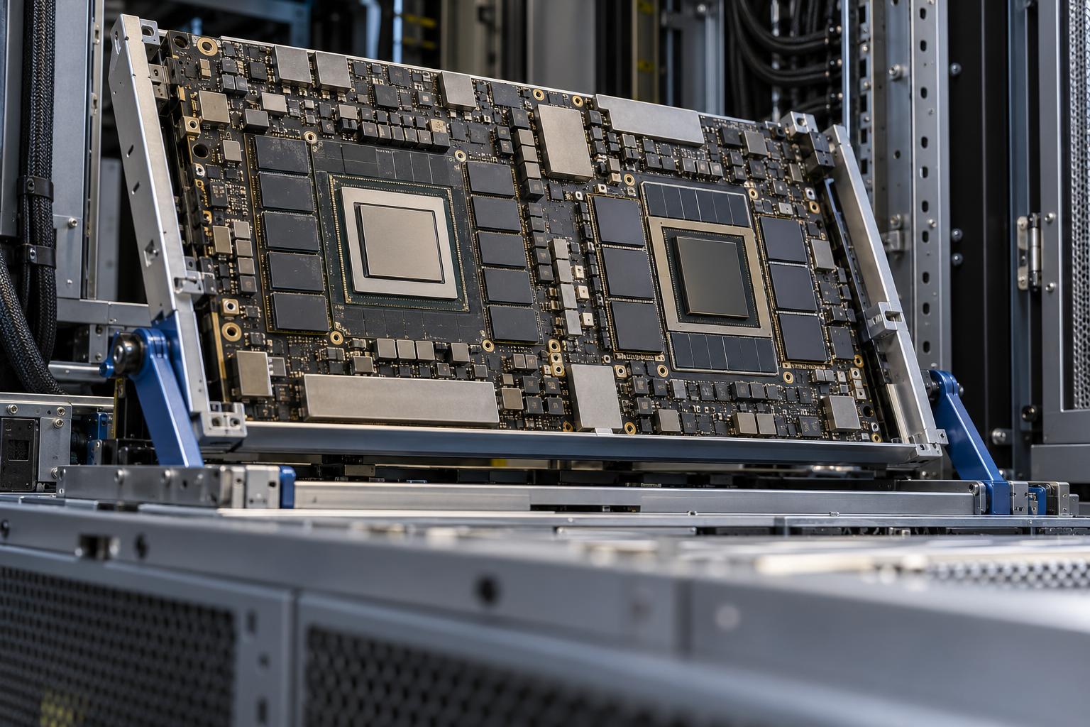
The GH200 Grace Hopper Superchip is one module carrying an NVIDIA Grace CPU (72 Arm Neoverse V2 cores) and a Hopper GPU, joined by NVLink-C2C instead of PCIe. NVIDIA's current Grace Performance Tuning Guide lists two GPU memory configurations, 96 GB HBM3 at up to 4 TB/s and 144 GB HBM3e at up to 4.9 TB/s, alongside up to 480 GB of LPDDR5X on the CPU side at up to 500 GB/s. The GH200 product page adds the top-line figures: a 900 GB/s coherent interface, "up to 624GB of combined CPU and GPU fast memory" (144 + 480 = 624), and "7X faster than PCIe Gen5." The GH200 datasheet linked from that page gives module power as "Configurable 450 to 1000W (Memory + CPU + GPU)" (900 to 2,000 W for GH200 NVL2) and LPDDR5X bandwidth of "up to 500GB/s".
Two caveats before using any of these numbers:
- Spec drift between documents. NVIDIA's 2022 architecture deep dive predates shipping silicon and quotes up to 512 GB of LPDDR5X at 546 GB/s and 96 GB of HBM3 at 3,000 GB/s. The tuning guide's and datasheet's 480 GB / 500 GB/s and 4 TB/s are the figures to plan against; the GB200 page's "up to 512 GB/s" describes Grace in GB200. Treat the 2022 blog as an architecture reference, not a datasheet.
- Installed LPDDR5X varies by system. The 480 GB figure is a maximum. The quad-GH200 nodes of the CSCS Alps supercomputer studied by Fusco et al. carry 96 GB of HBM3 and 128 GB of LPDDR5 per superchip, with only 120 GB available at the time of writing. Cloud instances differ again: CoreWeave's GH200 instance lists 96 GB GPU memory plus 480 GB of RAM, while Lambda's pricing page lists a GH200 instance with 96 GB VRAM and 432 GiB of RAM at $2.29 per GPU-hour (checked 2026-10-28). Confirm the memory population on the exact SKU you are quoting.
As of 2026-10-28 the product page still states "GH200 is currently available." We found no NVIDIA end-of-sale notice. GH200 is nonetheless a Hopper-generation part; the Blackwell vs Hopper comparison covers where it sits in the line-up.
NVLink-C2C in numbers
NVIDIA specifies NVLink-C2C at up to 900 GB/s total, 450 GB/s per direction, and describes it as "7x higher bandwidth than x16 PCIe Gen5 lanes" [1]. The ratio checks out against NVIDIA's own H100 spec, which lists "PCIe Gen5: 128GB/s" [2], i.e. 64 GB/s per direction:
450 GB/s per direction / 64 GB/s per direction = 7.03x
The link is hardware-coherent. The Grace CPU can cache GPU memory at cache-line granularity, and the link supports system-wide atomics. NVIDIA also quotes 1.3 picojoules per bit for C2C, which it says is more than 5x more energy-efficient than PCIe Gen 5 [1].
What independent measurement shows: on Alps, a Hopper kernel reading CPU-attached memory reached 93% of the 450 GB/s theoretical bound (419.5 GB/s in the paper's Figure 7), and writes reached 84%. Grace reading HBM across the same link managed only 53% [3]. The GPU is the better consumer of the link, which is the direction that matters for inference.
Memory pools and the bandwidth hierarchy
From the GPU's point of view a GH200 has three tiers. Bandwidths below are spec figures from the Grace tuning guide and the 2022 blog.
| Tier | Capacity (per superchip) | Peak bandwidth seen by the GPU | Ratio vs HBM3 |
|---|---|---|---|
| HBM3 / HBM3e | 96 GB / 144 GB | 4 TB/s / 4.9 TB/s | baseline (HBM3e is 1.23x faster) |
| LPDDR5X via C2C | up to 480 GB | min(500 GB/s LPDDR5X, 450 GB/s C2C per direction) = 450 GB/s | 4,000 / 450 = 8.9x slower |
| Peer GH200 memory (multi-superchip nodes) | varies | NVLink-limited; Fusco et al. measured accesses that cross both C2C and NVLink "never go above 60% of theoretical bandwidth" | slower still |
Two points follow from the table.
- The GPU's ceiling on CPU memory is the link, not the DRAM. LPDDR5X can deliver 500 GB/s, but a GPU reading it is capped at 450 GB/s per direction.
- The CPU memory is shared. Under contention, "Bandwidth to local DDR is limited by the bandwidth of 500 GB/s that needs to be split between two PUs" [3]. CPU-side work, such as tokenization, a Python serving loop or a KV-offload manager copying blocks, competes with the GPU for the same LPDDR5X bandwidth.
Address translation and unified memory
Three mechanisms make CPU memory usable from the GPU without explicit copies:
- Address Translation Services (ATS). "ATS enables the CPU and GPU to share a single per-process page table", so GPU threads can dereference memory from plain
malloc[1]. The CUDA guide describes the same property: "Hardware-coherent systems such as NVIDIA Grace Hopper offer a logically combined page table for both CPUs and GPUs" [4]. - System-allocated memory is migratable. The runtime backs it with physical memory on first touch and can later move it [1]. The CUDA guide documents access counters, which track how often a GPU touches a page, as one driver of migration, plus
cudaMemAdvisepreferred-location hints andcudaMemPrefetchAsync. - Extended GPU Memory (EGM). EGM lets GPUs in an NVLink-switched system address other superchips' CPU memory: "EGM provides up to 150 TBs of system memory in a multi-node NVSwitch-connected system", accessed "at the minimum of GPU-GPU NVLink or NVLink-C2C speed" [1].
The allocator decides where memory lives. Fusco et al. tabulate the behaviour (CUDA 12.x, Alps software stack):
| Allocation API | Physical placement | GPU translation / page size | Automatic migration |
|---|---|---|---|
malloc, new, mmap | first touch | ATS, system page size (64 KB on Alps) | yes (CUDA ≥ 12.4) |
numa_alloc_onnode | NUMA node you specify | ATS | no |
cudaMalloc | HBM | GPU MMU, 2 MB | no |
cudaMallocManaged | first touch | GPU MMU (HBM) | yes |
cudaMallocHost / cudaHostAlloc | DDR | ATS | no |
Source: Table II of Fusco et al.. Each GH200 appears to Linux as two NUMA nodes, LPDDR5X with affinity to Grace and HBM with affinity to Hopper, so numactl and libnuma can target HBM directly.
Put weights in HBM and use LPDDR5X for state that is read rarely or in bulk, such as idle KV blocks, prefix caches and cold MoE experts.
Inference use cases that fit
1. KV cache offload. This is the strongest fit. NVIDIA reports that on an x86 H100 server, offloading the KV cache to CPU memory over 128 GB/s PCIe can improve TTFT by "up to 14x" compared with recomputing the cache from scratch. GH200 adds up to 2x more TTFT speedup over the x86-H100 offload case for Llama 3 70B in multiturn scenarios, rising from 1.2x at 1,024 input tokens to 2x at 7,168 [5]. These are vendor-published results with unstated batch sizes.
Worked example: KV capacity for Llama 3.1 70B. The model config lists 80 layers, 8 KV heads and a hidden size of 8,192 over 64 attention heads, so the head dimension is 128 [6]. At FP16:
KV bytes/token = 2 (K,V) x 80 layers x 8 heads x 128 dim x 2 bytes = 327,680 B
128K context   = 327,680 x 131,072 = 42.9 GB (40 GiB)
That matches NVIDIA's "about 40 GB" per 128K-token user [7]. With FP8 weights (~70 GB) on a 96 GB GH200, at most about 26 GB of HBM is left for KV and activations. That is roughly 79,000 tokens before activation overhead (26e9 / 327,680). A full 480 GB of LPDDR5X holds about 1.46 million tokens of the same cache (480e9 / 327,680). Restoring one 128K context then costs:
over C2C (450 GB/s):        42.9 GB / 450 GB/s = 95 ms
over PCIe Gen5 (64 GB/s):   42.9 GB / 64 GB/s  = 671 ms
These are theoretical floors and ignore software overhead. The ~576 ms difference is what NVIDIA's multiturn TTFT result is exploiting. For sizing the cache itself, see the KV cache calculator.
2. Models slightly larger than HBM. NVIDIA's 2025 post shows PyTorch running models that exceed GPU memory by switching to RMM managed memory (rmm.reinitialize(managed_memory=True) plus rmm_torch_allocator), citing Llama 3 70B (~140 GB in FP16) and Llama 4 Scout 109B (~218 GB). The post publishes no performance numbers for the spilled case [7]. vLLM exposes a portable version as --cpu-offload-gb, "a virtual way to increase the GPU memory size". Its help text warns that this "requires fast CPU-GPU interconnect" because part of the model is loaded from CPU memory in each forward pass [8].
3. Prefill-heavy or offline batch work. When batches are large, each weight byte read from LPDDR5X is reused across many tokens, so the slow tier costs less per token (see the batch arithmetic below).
Where it hurts: decode reading from LPDDR5X
Decode is memory-bound. Each step streams the active weights once. If a fraction f of those bytes sits in LPDDR5X, the effective bandwidth for a sequential layer-by-layer pass is roughly:
BW_eff = 1 / ((1 - f) / 4,000 + f / 450) [GB/s, HBM3 GH200, theoretical]
| Fraction of weights in LPDDR5X | Effective bandwidth | Share of HBM-only speed |
|---|---|---|
| 0% | 4,000 GB/s | 100% |
| 10% | 2,236 GB/s | 56% |
| 25% | 1,346 GB/s | 34% |
| 43% | 913 GB/s | 23% |
| 50% | 809 GB/s | 20% |
Our arithmetic from spec bandwidths, not a measurement.
Worked example: Llama 3 70B in FP16 (~140 GB) on a 96 GB GH200. Place 80 GB of weights in HBM, leaving room for KV and activations, and 60 GB in LPDDR5X:
HBM part:   80 GB / 4,000 GB/s = 20.0 ms
LPDDR part: 60 GB /   450 GB/s = 133.3 ms
Step floor:                      153.3 ms  -> <= 6.5 tokens/s per sequence
The same 70B in FP8 (~70 GB) fits in HBM entirely: 70 / 4,000 = 17.5 ms, a ceiling of about 57 tokens/s. Here 43% of the bytes produce 87% of the step time (133.3 / 153.3). At batch 32 the 153 ms step yields up to ~209 aggregate tokens/s. That suits offline jobs, but every interactive user still waits at least 153 ms between tokens.
Fusco et al. ran Llama2-7B and 13B through Hugging Face generate with weights deliberately placed in DDR versus HBM. They found that memory access speed "plays a fundamental role in the throughput", although the gap was "less dramatic" than in purely memory-bound synthetic kernels [3]. Those runs used small models at batch 1 on an early software stack (driver 535.129.03), so they illustrate the effect but do not size a deployment.
The practical rule: quantize before you spill. Put weights in HBM and use LPDDR5X for state that is read rarely or in bulk, such as idle KV blocks, prefix caches and cold MoE experts. The inference hardware sizing guide walks through the same bandwidth-bound reasoning for HBM-only systems.
Placement and NUMA control
- Pin hot data to HBM explicitly.
cudaMallocalways lands in HBM. System-allocated buffers land wherever first touch happens, so a CPU thread that initializes a buffer places it in LPDDR5X. UsecudaMemAdvisewith a preferred location,cudaMemPrefetchAsync, ornuma_alloc_onnodeon the HBM NUMA node [4][3]. - Watch automatic migration. On CUDA 12.4 and later, system-allocated pages can migrate automatically based on access counters. This helps steady-state placement, but it can move pages during a latency-sensitive run. Benchmark after warm-up and pin what matters.
- Keep the CPU off the LPDDR5X hot path. The 500 GB/s is shared between Grace and Hopper. In Fusco's noise experiments, Grace's HBM write bandwidth fell to 17% of theoretical under contention.
- Framework support is uneven. vLLM (v0.32.0, released 2026-10-18) has
--cpu-offload-gbfor weights and--kv-offloading-sizewithnativeorlmcachebackends for KV [8]. Neither option is GH200-specific. Measure them on GH200 rather than assuming C2C-aware behaviour.
GH200 vs H100, H200 and GB200
| H100 SXM | H200 SXM | GH200 (HBM3 / HBM3e) | GB200 Superchip | |
|---|---|---|---|---|
| GPUs per unit | 1 | 1 | 1 | 2 |
| GPU memory | 80 GB | 141 GB | 96 GB / 144 GB | 372 GB HBM3E (two GPUs) |
| GPU memory bandwidth | 3.35 TB/s | 4.8 TB/s | 4 TB/s / 4.9 TB/s | 16 TB/s (two GPUs) |
| CPU memory | host DIMMs (x86) | host DIMMs (x86) | up to 480 GB LPDDR5X, 500 GB/s | up to 480 GB LPDDR5X, up to 512 GB/s |
| CPU-GPU link | PCIe Gen5, 128 GB/s | PCIe Gen5, 128 GB/s | NVLink-C2C, 900 GB/s | NVLink-C2C (bandwidth not on GB200 page) |
| GPU-GPU NVLink | 900 GB/s | 900 GB/s | system-dependent | 3.6 TB/s per superchip |
Sources: H100, H200 (whose page carries a "Preliminary specifications" note), Grace tuning guide, GB200 NVL72, all checked 2026-10-28. The GB200 page names NVLink-C2C as the Grace-to-Blackwell link but gives no figure for it. NVIDIA's Blackwell architecture page describes Grace memory access "over a high-speed link—900 gigabytes per second (GB/s) of bidirectional bandwidth" in its decompression-engine section.
Ratios that matter for spill decisions (our arithmetic):
GH200 HBM3 : LPDDR5X  = 4,000 / 500  = 8x
GH200 HBM3e: LPDDR5X  = 4,900 / 500  = 9.8x
GB200 HBM3E: LPDDR5X  = 16,000 / 512 = 31x   (one Grace feeds two GPUs)
GB200 keeps the same pairing idea, but the CPU memory is a relatively smaller and slower tier there. One Grace and its 480 GB serve two Blackwell GPUs (240 GB each if split evenly), against 480 GB for one Hopper on GH200. GB200's case rests on its 72-GPU NVLink domain, not on CPU memory. The next generation doubles the link: the Vera CPU article covers second-generation NVLink-C2C at 1.8 TB/s.
Deployment and cluster notes
- GH200 NVL2. Two superchips joined by NVLink give "up to 288GB of high-bandwidth memory, 10 terabytes per second (TB/s) of memory bandwidth, and 1.2TB of fast memory" [9]. That is enough HBM to run a 70B FP16 model with TP=2 entirely in HBM.
- Quad GH200 nodes. On Alps, each node behaves as one NUMA system with 288 CPU cores and 4 GPUs. Each GH200 connects to the HPE Slingshot 11 fabric at 200 Gb/s [3]. Locality dominates: their NCCL results show "same-GH200 memory greatly outperforming peer access."
- Arm host. The CPU is aarch64. Container images, Python wheels, monitoring agents and any x86-only binaries in the serving stack need arm64 builds. Check this before procurement, not after delivery.
Buy/skip rubric
| Situation | GH200 fit |
|---|---|
| Long-context or multiturn chat where KV reuse is high and HBM evicts often | Strong: C2C makes KV reload roughly 7x cheaper than PCIe |
| Model fits in HBM after FP8/INT4 quantization | Neutral: you pay for LPDDR5X you barely use; compare against H200 on $/token |
| Interactive serving of a model that only fits by spilling weights to LPDDR5X | Weak: the per-token floor is set by 450 GB/s |
| Offline batch inference of oversized models | Acceptable: large batches amortize LPDDR5X reads |
| Large tensor-parallel training or serving across many GPUs | Look at NVL72-class systems instead |
| Stack with x86-only dependencies | Skip until ported |
- Long-context or multiturn chat with frequent KV reuse benefits from faster cache reloads.
- Offline batch inference can amortize LPDDR5X reads across larger batches.
- Interactive serving suffers when the model fits only by spilling weights into LPDDR5X.
- A serving stack with x86-only dependencies needs porting before deployment.
If quantization already puts the model in HBM, the article rates GH200 neutral and recommends comparing against H200 on $/token.
Benchmark checklist before purchase
- Confirm the SKU: HBM3 96 GB or HBM3e 144 GB, installed LPDDR5X capacity, and driver and CUDA versions (≥ 12.4 if you rely on automatic migration).
- Run a C2C read/write microbenchmark from the GPU to LPDDR5X. Expect results near the ~93% / 84% of 450 GB/s that Fusco et al. measured. Rerun it with a CPU load running to see the contention.
- Serve your model all-in-HBM (quantized) and record TTFT and ITL p50/p99 at your target concurrency.
- Repeat with weight spill (
--cpu-offload-gb) at 10%, 25% and 50%, and compare against the effective-bandwidth table above. - Repeat with KV offload enabled on a multiturn trace with realistic reuse. Measure TTFT on cache hits against recompute.
- Run the same traces on an x86 H100 or H200 node to measure the PCIe-offload baseline yourself rather than relying on vendor ratios.
- Record power at the wall per node and compute tokens per joule for each configuration.
GPU Smith can help design and run this kind of pre-purchase benchmark plan against your own workloads.
- 01Confirm hardware and link
Check installed memory and software versions, then measure GPU reads and writes to LPDDR5X with and without competing CPU load.
- 02Establish the HBM baseline
Serve the quantized model entirely in HBM and record TTFT and inter-token latency at the intended concurrency.
- 03Measure weight spill
Repeat with increasing weight offload and compare the results with the article's effective-bandwidth table.
- 04Measure KV reuse
Use a multiturn trace with realistic reuse and compare cache-hit TTFT against recomputation.
- 05Compare the PCIe baseline
Run the same traces on an x86 H100 or H200 node to measure the offload baseline directly.
- 06Measure energy efficiency
Record power at the wall for each node and calculate tokens per joule for every configuration.
Sources
- NVIDIA, "Grace Hopper Superchip" product page. https://www.nvidia.com/en-us/data-center/grace-hopper-superchip/ (accessed 2026-10-28)
- NVIDIA, Grace Performance Tuning Guide (GH200 specification table). https://docs.nvidia.com/grace-perf-tuning-guide/index.html (accessed 2026-10-28)
- NVIDIA Technical Blog, "NVIDIA Grace Hopper Superchip Architecture In-Depth," Nov 10, 2022. https://developer.nvidia.com/blog/nvidia-grace-hopper-superchip-architecture-in-depth/
- L. Fusco et al., "Understanding Data Movement in Tightly Coupled Heterogeneous Systems: A Case Study with the Grace Hopper Superchip," arXiv:2408.11556, Aug 2024. https://arxiv.org/abs/2408.11556
- NVIDIA, H100 Tensor Core GPU page. https://www.nvidia.com/en-us/data-center/h100/ (accessed 2026-10-28)
- NVIDIA, H200 Tensor Core GPU page. https://www.nvidia.com/en-us/data-center/h200/ (accessed 2026-10-28)
- NVIDIA, GB200 NVL72 page. https://www.nvidia.com/en-us/data-center/gb200-nvl72/ (accessed 2026-10-28)
- NVIDIA, Blackwell Architecture page. https://www.nvidia.com/en-us/data-center/technologies/blackwell-architecture/ (accessed 2026-10-28)
- NVIDIA Technical Blog, "Accelerate Large-Scale LLM Inference and KV Cache Offload with CPU-GPU Memory Sharing," Sep 5, 2025. https://developer.nvidia.com/blog/accelerate-large-scale-llm-inference-and-kv-cache-offload-with-cpu-gpu-memory-sharing
- NVIDIA Technical Blog, "NVIDIA GH200 Superchip Accelerates Inference by 2x in Multiturn Interactions with Llama Models," Oct 28, 2024. https://developer.nvidia.com/blog/nvidia-gh200-superchip-accelerates-inference-by-2x-in-multiturn-interactions-with-llama-models
- NVIDIA, CUDA Programming Guide, 4.1 Unified Memory. https://docs.nvidia.com/cuda/cuda-programming-guide/04-special-topics/unified-memory.html (accessed 2026-10-28)
- vLLM, Engine Arguments, v0.32.0 (
--cpu-offload-gb,--kv-offloading-size,--kv-offloading-backend). https://docs.vllm.ai/en/v0.32.0/configuration/engine_args/ (accessed 2026-10-28) - Meta Llama 3.1 70B
config.json(public mirror). https://huggingface.co/unsloth/Meta-Llama-3.1-70B/raw/main/config.json - CoreWeave, GH200 instance documentation. https://docs.coreweave.com/platform/instances/gpu/gd-1xgh200 (accessed 2026-10-28)
- Lambda, Pricing. https://lambda.ai/pricing (accessed 2026-10-28)
- NVIDIA, GH200 Grace Hopper Superchip datasheet (linked from the product page; (c) 2025). https://dam-cdn.nvd.orangelogic.com/AssetLink/tkno03fa645gb7f33w60rf200d330420.pdf (accessed 2026-10-28)
External Sources (9)
About
GPUSmith
Plan and build private AI compute with GPU Smith. We connect workload requirements with GPU hardware, networking, deployment and operating decisions so your infrastructure fits the work it must perform.
GPU Smith provides independent engineering and research for private AI infrastructure. We help technical buyers and operators reason about GPU workload sizing, hardware selection, procurement, deployment and inference operations, from the compute system to the networking, power and cooling requirements around it.
Start with the workload
Useful infrastructure decisions begin with the models, data, throughput, latency and operating constraints a team actually has. GPU Smith helps connect those requirements with system design and deployment choices. The goal is a privately controlled AI environment whose capacity and operational demands are understood before a purchasing decision.
Hardware and supplier research
Our public reference library covers GPUs, complete systems and networking components. The server-vendor directory and manufacturing research help teams investigate suppliers, compare options and follow sources behind technical claims. We distinguish manufacturer specifications from measured benchmarks and advertised capabilities from tested configurations. Reference pages are research resources, not a live inventory listing or a binding equipment quote.
Deployment and operations
GPU Smith's engineering scope includes infrastructure integration, networking, power, cooling and the practical operation of inference workloads. Our published articles explain the tradeoffs behind deployment, procurement and ongoing operations so teams can ask better questions and document decisions.
Work with GPU Smith
Explore the hardware library, GPU references, networking references and vendor research. Contact GPU Smith with your workloads and deployment constraints to discuss a project and confirm current scope, pricing and availability.
Inclusion of a manufacturer or product in our research does not imply a partnership, certification or endorsement.
Disclaimer
This document is provided for informational purposes only. No representations or warranties are made regarding the accuracy, completeness, or reliability of its contents. Any use of this information is at your own risk. GPUSmith shall not be liable for any damages arising from the use of this document. This content was generated with assistance from artificial intelligence tools, which may contain errors or inaccuracies. Readers should verify critical information independently. All product names, trademarks, and registered trademarks mentioned are property of their respective owners and are used for identification purposes only. Use of these names does not imply endorsement. This document does not constitute professional or legal advice. For specific guidance related to your needs, please consult qualified professionals.