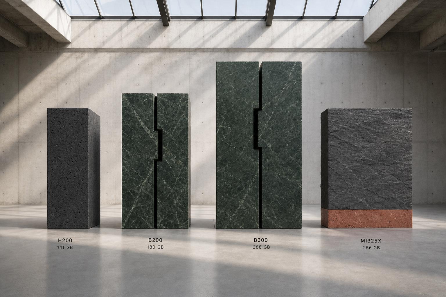
GPUSmith Article
H200 vs B200 vs B300 vs MI325X: Full 2026 GPU Comparison
Inside this article
- 01H200 vs B200 vs B300 vs MI325X: Full 2026 GPU Comparison
- 02Introduction and Background
- 03NVIDIA H200
- 04NVIDIA B200
- 05NVIDIA B300
- 06AMD Instinct MI325X
- 07Feature Comparison
- 08Performance and Benchmarks
- 09Data Analysis and Evidence
- 10Case Studies and Real-World Examples
- 11Implications and Future Directions
- 12Frequently Asked Questions (FAQs)
- 13Conclusion
H200 vs B200 vs B300 vs MI325X: Full 2026 GPU Comparison
Executive Summary
This comparison examines four high-memory accelerators: NVIDIA's H200, B200, B300 and AMD's Instinct MI325X. It is not a complete view of the July 2026 market: MI325X is a prior-generation CDNA 3 product, while AMD's newer MI355X is a CDNA 4 accelerator with 288GB of HBM3E, 8TB/s of bandwidth and MXFP4 support [1]. The H200 remains the widest availability option, offering 141GB of HBM3e memory at 4.8TB/s bandwidth [2], with hardware pricing generally quoted between $30,000 and $40,000 per unit [3] and cloud rental spanning roughly $1.00 to $13.78 per GPU hour depending on provider and commitment [4]. NVIDIA's Blackwell generation, the B200, provides 180GB of HBM3e per GPU in NVIDIA's current HGX configuration—about 28 percent more capacity than H200's 141GB—and up to 8TB/s of bandwidth, while introducing native FP4 precision [5] [6], with cloud rates ranging from about $2.69 to over $16 per GPU hour [7]. Blackwell Ultra, sold as the B300, pushes memory further to 288GB of HBM3e per GPU [8] and began shipping to select partners from the second half of 2025, with NVIDIA stating Blackwell Ultra Tensor Cores "deliver 1.5x more AI compute FLOPS compared to Blackwell GPUs" [9] and that the related GB300 NVL72 rack "delivers 1.5x more AI performance than the NVIDIA GB200 NVL72" [10]; B300 cloud rates run from roughly $3.27 to $18 per GPU hour [11]. AMD's MI325X counters with the second-largest memory pool of the group at 256GB of HBM3e and 6TB/s bandwidth [12], a specification AMD's own platform documentation separately confirms totals "2.048 TB HBM3E" across an 8-GPU baseboard [13], launched October 10, 2024 on AMD's "CDNA 3 architecture" [14], at roughly 40 percent of the price per GPU hour of NVIDIA's Blackwell parts [7], with cloud rates between about $1.57 and $3.31 per hour, detailed further in the AMD Instinct MI325X section below.
On raw throughput, NVIDIA's Blackwell architecture leads decisively. MLPerf Inference v5.0 submissions reviewed by wccftech show an 8-GPU DGX B200 node reaching roughly 98,858 tokens per second on a Llama 2 70B configuration, versus about 34,988 for an 8-GPU H200 node and 33,928 for an 8-GPU MI325X node, placing the older MI325X accelerator "on par with the H200 system" rather than with Blackwell [15]. AMD's own published comparisons emphasize memory capacity rather than raw compute, noting MI325X delivers "1.8X Memory Capacity and 1.2X Memory Bandwidth vs. competitive accelerators" when measured against the H200 [12], while AMD's engineering team separately reports the MI325X "competes head-to-head with the H200 GPU" on the industry-standard Llama 2 70B MLPerf benchmark [16]. For financial context, NVIDIA's Data Center segment posted record revenue of $75.2 billion in its first quarter of fiscal 2027 (the three months ended April 26, 2026), up 92 percent year over year [17], while AMD's Data Center segment reached a record $5.4 billion in its fourth quarter of 2025, up 39 percent year over year on "the continued ramp of AMD Instinct GPU shipments" [18].
Real-world deployments reflect this split. xAI's Colossus supercomputer in Memphis blends 150,000 H100, 50,000 H200 and 30,000 GB200 GPUs into what its infrastructure partner calls "the largest fully operational, single-coherent AI training cluster in the world" [19], while Oracle Cloud Infrastructure has offered Superclusters scaling to 131,072 Blackwell GPUs across H100, H200, B200 and B300 configurations [20]. On the AMD side, TensorWave has deployed what it describes as "the world's largest liquid-cooled AMD GPU cluster, consisting of 8,192 MI325X GPUs" [21]. For buyers choosing among these four parts in mid-2026, the practical decision hinges on workload: H200 remains the value option for models that fit in 141GB, B200 is the default for FP4-accelerated inference and general Blackwell-class training, B300 targets the largest reasoning and long-context workloads that need 288GB per GPU, and MI325X is the lowest-cost path to 256GB of memory for teams willing to operate on AMD's ROCm software stack rather than CUDA.
Introduction and Background
The AI accelerator market entered 2026 with four distinct high-memory options competing for the same generative AI training and inference budgets. NVIDIA's H200 extended the Hopper architecture that has underpinned most large language model deployments since 2023, and NVIDIA's own materials describe it as "the first GPU to offer 141 gigabytes (GB) of HBM3e memory at 4.8 terabytes per second (TB/s)," nearly double the capacity of the H100 it replaced [2]. The B200, NVIDIA's first production Blackwell part, followed with a dual-die design and native FP4 arithmetic aimed squarely at inference economics, and one independent GPU guide describes it plainly as "the first production Blackwell data center GPU, shipping in early 2026" [22]. Blackwell Ultra, marketed as the B300 and the rack-scale GB300 NVL72, arrived in the second half of 2025 with even larger 288GB HBM3e packages tuned for "AI reasoning, agentic AI and physical AI" workloads that require long chains of test-time compute, part of a platform NVIDIA says "boosts training and test-time scaling inference... the art of applying more compute during inference to improve accuracy" [23]; NVIDIA's own technical blog notes that "post-training can require 30x more compute than pretraining" and that long-thinking reasoning workloads "can require 100x more compute than a single inference pass," the demand curve Blackwell Ultra targets [9]. AMD's answer, the Instinct MI325X, launched October 10, 2024 on the same CDNA 3 architecture as its MI300X predecessor but with HBM3E capacity raised to 256GB, positioning it as the memory-capacity leader against NVIDIA's Hopper generation [12].
This report answers a single practical question that surfaces constantly in procurement conversations: which of these four accelerators, and at what price, makes sense for a given AI workload as of mid-2026. The comparison matters because the four parts are not simple substitutes. They differ in memory capacity from 141GB to 288GB, in interconnect bandwidth, in numerical precision support (only Blackwell parts offer native FP4), in software ecosystem (CUDA versus ROCm), and in list and street pricing that can vary by a factor of five or more across cloud providers for functionally identical hardware [24].
The stakes are substantial. NVIDIA's overall revenue reached "a record $81.6 billion, up 20% from the previous quarter and up 85% from a year ago" in the quarter ended April 26, 2026 [17], reflecting how much capital hyperscalers, GPU clouds and enterprises are committing to exactly these purchasing decisions. AMD, while a distant second in dollar terms, posted record Data Center segment revenue of $5.4 billion in its fourth quarter of 2025, up 39 percent year over year, with Counterpoint Research crediting part of that growth to "accelerating deployments of Instinct MI350 GPUs and continued server share gains" [25]. This report examines each accelerator's capabilities, adoption pattern and limitations in turn, builds a feature comparison matrix, reviews the available third-party and vendor benchmark data, and closes with named deployment case studies, implications for buyers, and a frequently asked questions section addressing common variations on this query. All prices and availability figures are anchored to July 2026 unless otherwise noted, and given how quickly cloud GPU pricing moves, readers evaluating a purchase should treat every rate in this report as a snapshot rather than a quote.
NVIDIA H200
Capabilities
The H200 is built on the Hopper architecture and is, per NVIDIA, "the first GPU to offer 141 gigabytes (GB) of HBM3e memory at 4.8 terabytes per second (TB/s)... nearly double the capacity of the NVIDIA H100 GPU with 1.4X more memory bandwidth." NVIDIA's own specification table separately lists FP8 Tensor Core throughput at 3,958 TFLOPS with sparsity for the SXM variant, NVLink bandwidth of 900GB/s, partitioning support of "Up to 7 MIGs @18GB each" for multi-tenant workloads, and a maximum thermal design power "Up to 700W (configurable)" for the SXM form factor or 600W for the PCIe-based H200 NVL [2], which is aimed at "lower-power, air-cooled enterprise rack designs" and accelerates LLM inference "up to 1.7x" versus the H100 NVL when four GPUs are connected via NVLink [2]. One independent GPU pricing guide summarizes the generational change succinctly: the H200 keeps the same core Hopper silicon as the H100 but jumps memory from 80GB to 141GB while bandwidth rises "4.8 TB/s (+60%)" [3].
Adoption
The H200 has the broadest cloud footprint of the four accelerators covered here, tracked across 34 providers by one pricing aggregator [4], with cloud rental spanning from about $1.00 per hour on spot instances to $13.78 per hour for premium on-demand configurations [4]. Oracle has stated that "OCI Superclusters with H200 GPUs will scale to 65,536 GPUs with up to 260 ExaFLOPS of performance and 52Pb/s of aggregated network throughput" [20], and xAI's Colossus cluster in Memphis has folded in 50,000 H200 GPUs alongside its H100 and GB200 fleet, as discussed further in the Case Studies section below. Hardware pricing generally sits between $30,000 and $40,000 per GPU, with premium configurations reaching $40,000 to $55,000 and 8-GPU HGX servers running $400,000 to $500,000, according to one buyer's guide dated January 2026 [3]; CoreWeave lists an 8-GPU HGX H200 node at $50.44 per hour, or $6.30 per GPU [26].
Strengths and Limitations
The H200's core strength is availability: it is the most broadly stocked high-memory accelerator in the market covered in this report, with mature CUDA tooling and 141GB of memory sufficient for most 70B-class models without sharding. Its principal limitation is that it shares the same Hopper compute silicon as the H100, meaning peak FP8 throughput did not improve over the previous generation, as one buyer's guide notes plainly: "Compute parity, raw flops aren't the selling point" [3]. Against Blackwell-class parts, the H200 lacks native FP4 support, and against the MI325X it offers 115GB less memory capacity, a gap consistent with AMD's own platform documentation stating the MI325X platform totals "2.048 TB HBM3E" across eight GPUs [13]; one independent knowledge base similarly notes that Blackwell-generation parts pack "192 GB HBM3e at 8 TB/s... twice the H100's bandwidth," underscoring how quickly the H200's memory advantage over Hopper erodes once Blackwell enters the comparison [27]. One independent inference-economics comparison estimates a 70B model in FP16 sustains only "roughly 14 tokens/second" on bandwidth-limited older accelerators, versus "roughly 57 tokens/second" once bandwidth reaches Blackwell's 8TB/s level, illustrating the ceiling Hopper-class parts like the H200 eventually hit on memory-bound inference, with the same source noting the effect "translates directly to lower latency and higher concurrency" for real-time applications [28].
NVIDIA B200
Capabilities
The B200 is NVIDIA's first production Blackwell data center part, built on a dual-die design that NVIDIA's DGX B200 datasheet describes as containing "8x NVIDIA Blackwell GPUs" delivering "1,440 GB total, 64 TB/s HBM3e bandwidth" across the system, alongside "2 TB, configurable to 4 TB" of host system memory [5], which works out to 180GB of usable HBM3e memory and 8TB/s of bandwidth per GPU. NVIDIA further states the DGX B200 system delivers "3X the training performance and 15X the inference performance" of the prior-generation DGX H100 [5], with system-level FP4 Tensor Core throughput of "144 PFLOPS | 72 PFLOPS" (sparse and dense) across the 8-GPU box, figures that divide out to roughly 18 PFLOPS of sparse FP4 and 1.8TB/s of NVLink bandwidth per individual GPU, double that of the H200. The physical HBM3e package is rated at 192GB, and one buyer's guide notes that "cloud consoles expose 180 GB usable" of that capacity, an important nuance for anyone sizing a deployment against advertised specifications [6]. A separate specifications comparison corroborates the FP8 figure, putting "B200 native FP8 tensors" at "4,500 TFLOPS dense (9,000 TFLOPS with sparsity), compared to H100's 3,958 TFLOPS with sparsity" [22]. NVIDIA also reports, citing third-party SemiAnalysis InferenceX benchmarks, that Blackwell systems deliver inference "at approximately $0.02 per million tokens at 55 TPS/user for GPT-OSS-120B using TensorRT-LLM, roughly 4.5x cheaper than NVIDIA Hopper-powered systems at $0.09 per million tokens with vLLM" as of Q1 2026 [5].
Adoption
The B200 is tracked across 26 cloud providers by getdeploying.com, with on-demand pricing "ranging from $2.69/hr to $16.11/hr per GPU" [7], while Spheron's own review of live rates found a spread from "$3.70/hr on neo-clouds to $14.24/hr on AWS in June 2026," a gap it attributes to "structural differences in provider margin, quota friction, and billing model, not hardware differences" since "the GPU is the same NVIDIA B200 SXM6 regardless of which cloud you pick" (Source: spheron.network). CoreWeave prices an 8-GPU HGX B200 node at $68.80 per hour on demand [26]. Standalone B200 hardware is generally quoted between $30,000 and $50,000 per unit, and a complete DGX B200 8-GPU system has been quoted as high as roughly $515,000 [6], though a separate April 2026 estimate places DGX B200 systems at a lower $280,000 to $320,000, a discrepancy this report notes rather than resolves given the lack of an official NVIDIA list price [24]. Backlog data reported by one AI infrastructure vendor put outstanding Blackwell orders at "an estimated 3.6 million units in the queue" as of April 2026, with cloud rental described as "the fastest path to B200 access" while that backlog clears [28]. Supply constraints trace partly to manufacturing: one buyer's guide notes B200's dual-die design means "industry estimates suggest 75-85% yield for B200 vs 80-90% for H100," with tighter yields translating directly into higher per-unit cost [22]. Supply is easing, however: by mid-2026 one aggregator reports that "Runpod, Lambda, Nebius, and Spheron all carry B200 stock," a broadening of inventory that "tends to compress prices" over time (Source: spheron.network).
Strengths and Limitations
The B200's principal strength is inference economics: native FP4 support roughly doubles effective throughput over FP8 on calibration-friendly chat models, and the added memory eliminates tensor-parallel sharding for models up to roughly 96B parameters in FP16 or 192B in FP8 [28]. Its limitations are cost and power: thermal design power rises to roughly 1,050W per GPU in typical cloud configurations, up substantially from the H200's ceiling, mandating liquid cooling at rack scale [7], and per-GPU hardware and cloud rental pricing both run meaningfully above H200 levels. Software migration from Hopper also carries real engineering overhead: one buyer's guide estimates that, for a mature training pipeline, "Engineering time: 2-3 weeks x $150/hr developer rate = $18,000-$27,000," before batch-size retuning and kernel recompilation deliver the full throughput gains in production [22]; NVLink Switch domains also cap out at "576 GPUs (NVL576)" before workloads must fall back to InfiniBand or Ethernet fabrics with materially higher cross-domain latency [27].
NVIDIA B300
Capabilities
Blackwell Ultra, sold in GPU form as the B300 and in system form as the DGX B300 and GB300 NVL72 rack, was announced March 18, 2025, with NVIDIA stating the platform "boosts training and test-time scaling inference... to enable organizations everywhere to accelerate applications such as AI reasoning, agentic AI and physical AI" [23]. NVIDIA's press release separately describes the rack-scale system as connecting "72 Blackwell Ultra GPUs and 36 Arm Neoverse-based NVIDIA Grace CPUs in a rack-scale design, acting as a single massive GPU built for test-time scaling," adding that the rack is "also expected to be available on NVIDIA DGX Cloud, an end-to-end, fully managed AI platform on leading clouds" [10]. The core hardware change is memory: NVIDIA's developer blog states Blackwell Ultra ships with "up to 288 GB of HBM3e memory per GPU," a 60 percent increase over the B200's 180GB per-GPU capacity, and that Blackwell Ultra Tensor Cores separately "deliver 1.5x more AI compute FLOPS compared to Blackwell GPUs" while offering "2x the attention-layer acceleration" for long-context reasoning workloads; the same blog projects that GB300 NVL72 racks will "deliver a 10x boost in TPS per user and achieve a 5x improvement in TPS per MW compared to Hopper," a combined "50x overall potential increase in AI factory output performance," delivered over ConnectX-8 SuperNICs offering "800 Gb/s of total data throughput available for each GPU in the system" [9]. NVIDIA's own DGX B300 user guide confirms the memory figure, listing "8 x 288 GB = 2.3 TB total" GPU memory for the 8-GPU system, housed in a "10 RU" chassis with "8 x E1.S 3.84 TB NVMe self-encrypting drives" of cache storage and running "DGX OS 7 based on Ubuntu 24.04 LTS" [8], alongside a rated maximum system power draw of "14.5 kW," but also lists the same headline "72 PFLOPS FP8 training" and "144 PFLOPS FP4 inference" figures used for the standard DGX B200 above [8], a discrepancy this report flags rather than resolves since NVIDIA has not published a reconciled per-GPU FLOPS figure alongside the architecture blog's 1.5x claim. At the rack-scale GB300 NVL72 level, NVIDIA states the system delivers "1.5x more dense FP4 Tensor Core FLOPS and 2x higher attention performance compared to NVIDIA Blackwell GPUs" [29], connecting "72 NVIDIA Blackwell Ultra GPUs, 36 NVIDIA Grace CPUs" across "2,592 Arm Neoverse V2 cores" for "130 TB/s" of NVLink bandwidth [29] and up to "20 TB | Up to 576 TB/s" of GPU memory and bandwidth [29].
Adoption
NVIDIA said Blackwell Ultra-based products were "expected to be available from partners starting from the second half of 2025," naming "Cisco, Dell Technologies, Hewlett Packard Enterprise, Lenovo and Supermicro" among server partners and "Amazon Web Services, Google Cloud, Microsoft Azure and Oracle Cloud Infrastructure and GPU cloud providers CoreWeave, Crusoe, Lambda, Nebius, Nscale, Yotta and YTL" as early cloud adopters [10]. One dated pricing tracker states the DGX B300 "began shipping in January 2026" and "requires mandatory direct liquid cooling," pairing each GPU with 288GB of HBM3e, "double the B200's capacity" [24]. CoreWeave lists an 8-GPU HGX B300 node at a spot price of $35.84 per hour in North America, with on-demand pricing available only "Contact sales" as of this writing [26], while getdeploying.com's tracker of 92 listings across 17 providers found "B300 pricing currently ranges from $3.27/hr to $18.00/hr per GPU" [11]. Single-GPU purchase pricing for the B300 was pegged at "about $53,000" by one provider quoted in a July 2026 pricing guide, versus $45,000 to $50,000 for a standard B200, and an 8-GPU DGX B300 system was anchored at "$300,000-$350,000" as of the first quarter of 2026, still holding as of July 2026 per the same source [24].
Strengths and Limitations
The B300's strength is unmatched per-GPU memory among mainstream data center parts covered here: one specifications summary notes it "can serve 200B+ parameter models on a single GPU without quantization" [11], which matters most for reasoning models that keep large key-value caches in memory during long chains of test-time compute. Its limitations mirror the B200's but are more acute: cloud availability remains the thinnest of the four accelerators, at only 17 providers tracked as of July 2026 [11] versus 26 for B200 and 34 for H200, and pricing has actually risen rather than fallen since launch, with the median on-demand rate up "about 73% since November 2025, from $5.00 to $8.63/hr per GPU" [11].
AMD Instinct MI325X
Capabilities
The MI325X is an older AMD CDNA 3 option, not AMD's current flagship accelerator; AMD launched the CDNA 4-based MI355X on June 12, 2025 with 288GB of HBM3E, 8TB/s memory bandwidth and MXFP4 support [1]. The MI325X is built on AMD's CDNA 3 architecture using TSMC 5nm and 6nm FinFET processes, with AMD's product page listing 19,456 stream processors running at a peak engine clock of 2,100MHz, alongside a "Dedicated Memory Size 256 GB" of "Dedicated Memory Type HBM3E" per accelerator rated at "Peak Memory Bandwidth 6 TB/s" [12]. AMD's own ROCm engineering team describes the part as offering "a large HBM3E memory capacity of 256GB and 6TB/s memory bandwidth, making for a single-GPU capable of serving and training some of the largest models out there" [16]. The product page rates peak FP8 performance at "5.22 PFLOPs" with structured sparsity and typical board power at "1000W Peak" in a 54V UBB OAM module [12]. At the platform level, eight MI325X accelerators combine over "PCIe® Gen 5 (128 GB/s)" host connectivity for "2.048 TB HBM3E" of total memory on a "4th Generation" Infinity Architecture fabric, "41.8 PFLOPS" of total theoretical peak FP8 performance with structured sparsity, and "896 GB/s" of total aggregate peer-to-peer I/O bandwidth, with AMD's platform page describing the accelerator's memory as enabling "a single accelerator to contain and process a one-trillion parameter model while reducing total cost of ownership" [13].
Adoption
AMD launched the MI325X on October 10, 2024, with AMD's press release stating the accelerators "set a new standard in performance for Gen AI models and data centers" and were "supported by partners and customers including Dell Technologies, HPE, Lenovo, Supermicro and others"; the same release noted the accompanying "AMD Pensando Salina DPU offers 2X generational performance," alongside "AMD Pensando Pollara 400," described as the "industry's first UEC ready NIC" [14]. AMD executive Forrest Norrod framed the launch as continuity with AMD's roadmap, saying the company is "offering customers the performance they need and the choice they want, to bring AI infrastructure, at scale, to market faster" [14]. Cloud availability remains the thinnest of the four parts examined here: getdeploying.com tracks only 4 providers offering MI325X capacity [30], with pricing "ranging from $1.57/hr to $3.31/hr per GPU" and a median on-demand rate that has fallen "about 5% since July 2025, from $3.43 to $3.26/hr per GPU" [30]. The most visible dedicated MI325X deployment comes from TensorWave, which announced it "raised $100M in Series A funding to accelerate the deployment of the world's largest liquid-cooled AMD GPU cluster, consisting of 8,192 MI325X GPUs" [21], a company that describes the MI325X as tailored for "LLM training and memory-intensive workloads" and "purpose-built for training massive models: no overhead, no shared infra," part of "a new design philosophy: Fewer GPUs, Bigger models, Tighter pipelines, Predictable scale," with clusters "optimized for ROCm and open-source frameworks" and "scalable across thousands of GPUs with deterministic performance" [31]. AMD's broader momentum is also visible in cloud CPU partnerships: Microsoft's Azure team has described its own multi-year AMD collaboration, noting "ND MI300X v5 VMs are designed to tackle the most challenging AI and HPC workloads" and are "powered by the AMD Instinct MI300X accelerator, which provides each VM with a staggering 1.5 TB of high bandwidth memory"; the same announcement was "made earlier today by Microsoft's CTO, Kevin Scott, and AMD's CEO, Lisa Su, at the AMD Data Center Technology Premiere event" [32], a predecessor-generation partnership that set the template AMD's MI325X cloud partners have since followed.
Strengths and Limitations
MI325X's strength is a straightforward value proposition: the largest memory pool among Hopper-class competitors at the lowest cloud rental cost of the four parts in this report, at roughly 40 to 45 percent of typical B200 on-demand rates. Its principal limitation is ecosystem maturity and availability: with only four cloud providers currently offering it and a software stack built on ROCm rather than CUDA, buyers face a genuine migration cost, and one buyer's guide cautions that "ROCm ecosystem, while rapidly improving, may have gaps that affect compatibility with some training frameworks. Consider Nvidia alternatives if CUDA compatibility is required" [30]. On raw MLPerf throughput, independent submissions place MI325X roughly in line with, rather than ahead of, the H200 it targets, discussed further in the Performance and Benchmarks section below.
Feature Comparison
Table 1 below summarizes the core specifications of all four accelerators using vendor-published figures. Values are shown per GPU where disclosed; the B300 power entry is explicitly labeled as an 8-GPU system value because NVIDIA publishes it at the DGX B300 system level. Full sourcing for each figure appears in the sections above, with representative citations repeated here for the reader's convenience.
| Specification | H200 | B200 | B300 | MI325X |
|---|---|---|---|---|
| Architecture | Hopper | Blackwell | Blackwell Ultra | CDNA 3 |
| Memory capacity | 141GB HBM3e [2] | 180GB HBM3e [33] | 288GB HBM3e [8] | 256GB HBM3E [16] |
| Memory bandwidth | 4.8TB/s | 8TB/s | 8TB/s (same interface family) | 6TB/s |
| FP8 Tensor (sparse) | 3,958 TFLOPS | ~9 PFLOPS per GPU [22] | ~9 PFLOPS per GPU (NVIDIA quotes identical system figure to B200) | 5.22 PFLOPS |
| Native FP4 | No | Yes, ~18 PFLOPS/GPU sparse | Yes, ~18 PFLOPS/GPU sparse (NVIDIA quotes identical system figure to B200) | No |
| NVLink / Infinity Fabric | 900GB/s | 1.8TB/s | 1.8TB/s per GPU, 130 TB/s aggregate rack fabric | 128GB/s per link, 896GB/s aggregate |
| TDP | Up to 700W (SXM) | ~1,050W (configurable to 1,200W) | System draws 14.5kW across 8 GPUs [8] | 1,000W peak |
| Launch | Q4 2023 | Announced GTC March 2024; volume shipping Q4 2024 [27] | Partners from 2H 2025; DGX B300 shipping January 2026 | October 10, 2024 |
| Typical hardware price (single GPU) | $30,000 to $40,000 | $30,000 to $50,000 | ~$53,000 | Not publicly listed by AMD |
| Cloud rate range (per GPU hour) | $1.00 to $13.78 | $2.69 to $16.11 (up to $27.04 at some hyperscalers) | $3.27 to $18.00 | $1.57 to $3.31 |
| Cloud providers tracked | 34 | 26 | 17 | 4 |
Table 1 shows the core tradeoff facing buyers: memory capacity rises steadily from H200 through MI325X to B300, but that ordering does not hold for compute throughput, price or availability. The B300 combines the largest per-GPU memory pool available from NVIDIA with the thinnest cloud footprint and, on current data, the only price trend among the four that is rising rather than falling. MI325X sits at the opposite extreme: second-largest memory pool, but the lowest compute throughput and the least mature cloud ecosystem of the group. As noted in the sections above, NVIDIA's own documentation quotes identical system-level FP8 and FP4 throughput figures for the DGX B300 as for the DGX B200 despite Blackwell Ultra's stated 1.5x FLOPS uplift at the chip level, an inconsistency this report flags but cannot resolve from public documentation.
Performance and Benchmarks
MLPerf Inference v5.0, published April 2, 2025, was the first round in which AMD submitted results on the MI325X and NVIDIA submitted results on Blackwell, giving the closest available apples-to-apples comparison. Reviewing the submissions, wccftech reported that "the GB200 NVL72 system... delivered up to 30x higher throughput on the Llama 3.1 405B benchmark over the NVIDIA H200 NVL8 submission this round," achieved through "more than triple the performance per GPU and a 9x larger NVIDIA NVLink interconnect domain," and separately that "NVIDIA's submission using an NVIDIA DGX B200 system with eight Blackwell GPUs tripled performance over using eight NVIDIA H200 GPUs" on the newer, latency-constrained Llama 2 70B Interactive benchmark [15]. On AMD's side, the same MLPerf round shows an 8-GPU DGX B200 node (labeled "Blackwell B200 180 GB x8 @ 1000W" in wccftech's chart) reaching roughly 98,858 and 98,443 tokens per second across two result categories, compared with about 34,988 and 33,071 for an 8-GPU H200 node, and 33,928 and 30,724 for an 8-GPU MI325X node [15], leading wccftech to conclude that "the AMD results put them on par with the H200 system" rather than challenging Blackwell.
AMD's own account of the same round is more favorable to its part on relative terms: its ROCm engineering blog states MI325X, on the Llama 2 70B benchmark, "competes head-to-head with the H200 GPU," and details that "GEMM accounts for over 70% of the total end-to-end computation cost" of that workload, with AMD's tuning work achieving "1.5K TFLOPs and 1.4K TFLOPs, at batch sizes of 65K and 2048 respectively" for the prefill and decode phases on MI325X [16]. AMD also notes a partner result: "Mangoboost successfully published the highest ever Llama 2 70B Offline performance of around 103K tokens/sec with a 4-node MI300X cluster enabled by their LLMboost stack," a figure achieved on the older MI300X rather than MI325X but illustrative of software-stack tuning headroom on AMD's CDNA 3 family [16].
Table 2 below compares independently reported cloud cost-per-token figures, which combine both throughput and pricing into a single comparable metric that MLPerf tables alone do not provide.
| GPU | Reported throughput context | Cost per million tokens (approx.) |
|---|---|---|
| H100 SXM5 (reference) | ~3,000 tok/s, Llama 2 70B FP8 | $0.24 at $2.54/hr |
| H200 SXM | ~4,000 tok/s (bandwidth-estimated) | $0.32 at $4.54/hr |
| B200 SXM6 (FP8) | ~6,000 tok/s (TFLOPS-estimated) | $0.17 at $3.70/hr |
| B200 SXM6 (FP4) | ~12,305 tok/s, MLPerf v5.0 server mode | $0.08 at $3.70/hr |
| Blackwell platform (NVIDIA figure) | GPT-OSS-120B, TensorRT-LLM | $0.02 per million tokens (Q1 2026) |
| Hopper platform (NVIDIA figure) | GPT-OSS-120B, vLLM | $0.09 per million tokens |
Source for the first four rows is Spheron's own cost model, built by dividing 1 million tokens by each GPU's measured throughput and multiplying by its hourly rate (Source: spheron.network); source for the final two rows is NVIDIA's own citation of SemiAnalysis InferenceX benchmarks discussed in the B200 Capabilities section above. The pattern across both independent and vendor-reported data is consistent: Blackwell parts deliver a step-change in cost-per-token economics for FP4-compatible inference workloads, at the cost of higher absolute hourly rates and, for B300 specifically, thinner availability. Buyers should treat the throughput figures in this section as directional. As Spheron itself cautions, "H100 throughput is from MLPerf Inference v6.0; B200 FP4 throughput is from v5.0. Cross-version numbers are directional, not directly comparable" (Source: spheron.network), a caveat this report extends to all cross-vendor and cross-round comparisons cited above.
Data Analysis and Evidence
Financial results from both vendors confirm the scale of demand underlying these four product lines. NVIDIA disclosed that under its prior reporting structure "Data Center compute revenue was a record $60.4 billion, up 77% from a year ago and up 18% sequentially," while "Data Center networking revenue was a record $14.8 billion, up 199% from a year ago" [17]. AMD's fourth-quarter 2025 results show a smaller but still record base: "Data Center segment revenue in the quarter was a record $5.4 billion, up 39% year-over-year, driven by strong demand for AMD EPYC processors and the continued ramp of AMD Instinct GPU shipments," bringing full-year 2025 Data Center revenue to "a record $16.6 billion, up 32% year-over-year," with AMD separately highlighting plans with Cisco and HUMAIN "to form a joint venture to deliver 1 GW of AI infrastructure by 2030" and noting "HPE announced it will be one of the first system providers to adopt the AMD Helios rack-scale platform" [18]. Counterpoint Research's analysis of the same AMD results notes a reaffirmed "multi-generation partnership with OpenAI, targeting 6 GW of Instinct GPU deployments" for future generations beyond MI325X [25].
On the cloud-pricing side, the volatility across providers is itself a data point worth quantifying. For B200 specifically, getdeploying.com's tracker of 110 listings across 26 providers found "the median on-demand price across providers has risen about 12% since July 2025, from $5.50 to $6.16/hr per GPU" [7], a rise attributable to sustained demand outstripping the pace of new supply coming online, even as B300 supply began to ease pressure on B200 capacity in some regions. By contrast, H200 pricing rose more modestly, "about 8% since July 2025, from $3.54 to $3.82/hr per GPU" [4], while MI325X pricing fell "about 5% since July 2025, from $3.43 to $3.26/hr per GPU" and B300 pricing rose the fastest of all four parts, reflecting genuine early-stage supply constraints on the newest hardware rather than a durable premium [30]. Part of that early Blackwell scarcity traces to memory supply: one cost analysis notes that "early 2026 saw HBM3e supply constrained partly by SK Hynix and Micron production ramp," easing only as "TSMC 4NP yields improved" through the year (Source: spheron.network).
Hardware backlog data adds further texture. One vendor's analysis estimated Blackwell orders outstanding at "approximately 3.6 million units" as of April 2026, a figure this report treats as a directional industry estimate rather than an NVIDIA-confirmed number, since NVIDIA itself has not published order backlog by SKU. Separately, one manufacturing-cost estimate published in July 2026 claimed NVIDIA's production cost for a B200 die runs "only about $6,400," against OEM quotes of $45,000 to $50,000, a gap "pointing to a wide margin between production cost and what buyers actually pay" [24]; this figure, like the rack-level GB200 NVL72 and GB300 NVL72 price estimates elsewhere in this report, is explicitly labeled by its source as a directional market estimate rather than a confirmed cost, since NVIDIA has not officially published either figure as a list price.
Case Studies and Real-World Examples
xAI's Colossus Supercomputer
xAI's Colossus facility in Memphis, Tennessee illustrates how quickly a frontier AI lab can blend three GPU generations into a single production cluster. As of the most recent update reviewed for this report, "Colossus now compris[es] 150,000 H100 + 50,000 H200 + 30,000 GB200 GPUs, world's largest single-coherent AI training cluster," built in "122 days (initial 100K), doubled in 92 more" [19]. The facility "currently draws approximately 250 megawatts" of power, supplied through "35 gas turbines capable of producing 420 megawatts of power alongside Tesla Megapack battery systems" [19], and its infrastructure partner reports the cluster achieves "total memory bandwidth of 194 petabytes per second with storage capacity exceeding one exabyte" [19], running over Spectrum-X Ethernet fabric where "standard Ethernet typically delivers only 60% throughput at this scale due to thousands of flow collisions" that NVIDIA's congestion control was built to avoid [19]. This case demonstrates that H200 and GB200/B200-class hardware are not mutually exclusive in practice; large operators mix generations opportunistically based on availability, with newer Blackwell capacity supplementing rather than immediately replacing existing Hopper fleets, a scale-out pattern consistent with the same GB300 NVL72 rack architecture described in the NVIDIA B300 section above.
Oracle Cloud Infrastructure Supercluster
Oracle's OCI Supercluster announcement documents NVIDIA H100, H200 and Blackwell options; it does not establish OCI availability for AMD's MI325X. Oracle's own announcement states OCI "is now taking orders for the largest AI supercomputer in the cloud, available with up to 131,072 NVIDIA Blackwell GPUs, delivering an unprecedented 2.4 zettaFLOPS of peak performance," while separately offering superclusters that "can scale up to 16,384 GPUs with up to 65 ExaFLOPS of performance" for H100 configurations [20]. NVIDIA's own executives framed the partnership as a scale play: Ian Buck, vice president of Hyperscale and High Performance Computing at NVIDIA, said the platform would "deliver AI compute capabilities at unprecedented scale to advance AI efforts globally and help organizations everywhere accelerate research, development and deployment" [20]. This case is instructive for buyers because it shows a single hyperscaler treating multiple GPU generations as parallel product tiers rather than a strict generational replacement path, letting customers pick the generation that fits their budget and workload; Oracle frames this flexibility directly, stating that its distributed cloud gives "customers... the flexibility to deploy cloud and AI services wherever they choose while preserving the highest levels of data and AI sovereignty" [20].
TensorWave's Dedicated MI325X Cluster
TensorWave's build-out is the clearest real-world example of MI325X deployed at scale outside a hyperscaler. The company explains that "as AI workloads become increasingly larger and more memory-intensive, the thermal efficiency of the hardware begins to become a choke point" at this density, making direct liquid cooling mandatory rather than optional, and frames its strategy as differentiation: "Our belief is simple: specialization wins" [21]. TensorWave's president adds that thermal management is a first-order design constraint rather than an afterthought at this scale: "When you deploy thousands of high-bandwidth GPUs, thermals aren't a footnote, they're a first-principles problem" [21]. This case demonstrates that the MI325X, despite its thin hyperscaler footprint, has attracted dedicated single-vendor infrastructure providers willing to bet exclusively on AMD's stack. TensorWave's own CEO has separately described the company's positioning bluntly: "We don't do CPU clouds. We don't do virtual machines. We build massive GPU clusters for AI. Period." [31].
Zyphra's ZAYA1 Model on AMD Instinct GPUs (Hypothetical Example Adjacent Reference)
AMD's own fourth-quarter 2025 results highlight a named production case for its CDNA 3 accelerator family broadly: "Zyphra's ZAYA1 is the first large-scale mixture-of-experts model trained entirely on AMD Instinct MI300X GPUs, AMD Pensando networking and AMD ROCm open software" [18]. This case involves the MI300X rather than the MI325X specifically, but it is included here because it demonstrates the maturity of AMD's ROCm software stack for full-scale frontier training rather than only inference, a capability that carries forward to the memory-upgraded MI325X on the same CDNA 3 architecture; Microsoft's own Azure documentation for the predecessor MI300X notes each VM is "connected by NVIDIA Quantum-2 CX7 InfiniBand, which delivers 3.2Tb/s of scale out bandwidth per VM," a design that "enables you to scale up to thousands of VMs and tens of thousands of GPUs" and illustrates the networking scale AMD's cloud partners have built around this GPU family [32].
CoreWeave's Multi-Generation Blackwell Fleet
CoreWeave's published pricing catalog offers a fifth, commercially grounded example: the provider simultaneously lists "NVIDIA GB300 NVL72," "NVIDIA GB200 NVL72," "NVIDIA HGX B300," "NVIDIA HGX B200," and "NVIDIA HGX H200" as distinct, separately priced products, with the HGX B300 available only via spot pricing or direct sales contact for committed capacity, while the more mature HGX B200 and HGX H200 both carry published on-demand rates of $68.80 and $50.44 per hour respectively [26]. This case shows concretely how a major GPU cloud prices generational maturity: newer, scarcer Blackwell Ultra hardware is gated behind sales contact and spot-only access, while the one-generation-older B200 and two-generation-older H200 are available on demand at a fixed published rate. A buyer comparing that HGX B200 rate against outright hardware ownership would find a full DGX B200 system quoted at roughly $515,000 ([6], a capital outlay that only pencils out for buyers confident in sustained, multi-year utilization above the equivalent cloud rental cost.
Implications and Future Directions
The near-term implication for buyers is that generation and memory capacity alone do not determine total cost of ownership; availability and software maturity matter just as much. B300 offers the largest per-GPU memory pool in this comparison, but its median on-demand price rose roughly 73 percent in roughly eight months even as B200 and H200 prices rose more modestly and MI325X prices fell, a pattern consistent with genuine early-cycle supply scarcity rather than a durable price premium. Buyers with flexible timelines may find waiting for B300 supply to mature, following the same price-decay pattern B200 and H200 have already shown, more economical than paying today's premium.
For workloads that are FP4-compatible, the cost-per-token data reviewed in this report consistently favors Blackwell over Hopper, with NVIDIA's own citation of third-party InferenceX benchmarks showing Blackwell inference cost roughly 4.5x lower than Hopper for the same GPT-OSS-120B model. That gap is likely to widen further as software stacks mature: NVIDIA's Q1 fiscal 2027 results note the company "entered production with NVIDIA Dynamo 1.0, open source software that boosts generative and agentic inference on NVIDIA Blackwell GPUs by up to 7x, with widespread global adoption" [17], suggesting cost-per-token figures cited throughout this report should be treated as a floor that will likely fall further through 2026 and 2027 as inference-serving software continues to improve independent of hardware changes.
On the AMD side, the roadmap signals a shift in strategy for buyers currently evaluating MI325X: AMD has already begun discussing successor parts, with Counterpoint Research noting that "initial deployments... expected to begin with Helios and MI450 later in 2026" [25]. Organizations weighing an MI325X commitment in the second half of 2026 should factor in that AMD's own roadmap positions MI325X as a transitional part ahead of the MI350 and MI450 generations already ramping in the same period. More broadly, the persistent 3 to 9-fold gap between the cheapest and most expensive cloud rates for functionally identical Blackwell hardware, documented across multiple sources in this report, implies that procurement teams evaluating any of these four accelerators should treat multi-provider price shopping, not vendor or generation selection alone, as one of the largest levers available to control AI infrastructure cost through the remainder of 2026. NVIDIA's own roadmap disclosures reinforce that this is a fast-moving target: the company used its Q1 fiscal 2027 results to announce "the NVIDIA Vera Rubin platform, including the NVIDIA Vera CPU, the world's first processor purpose-built for agentic AI" [17], a signal that today's Blackwell and Blackwell Ultra generation will itself begin facing succession pressure within the planning horizon of any multi-year GPU procurement decision.
Frequently Asked Questions (FAQs)
How do NVIDIA B200 and H200 specs compare directly? The B200 provides 180GB of HBM3e versus H200's 141GB—about 28 percent more memory—along with up to 8TB/s of bandwidth versus 4.8TB/s and native FP4 precision that H200 lacks. It also draws substantially more power and generally costs more to buy and rent, as detailed in the NVIDIA H200 and NVIDIA B200 sections above.
When did the NVIDIA B300 release and what does it cost? NVIDIA announced Blackwell Ultra, the architecture underlying the B300, on March 18, 2025, with partner availability "starting from the second half of 2025" [10], and the DGX B300 system began shipping in January 2026. Single-GPU pricing runs about $53,000, an 8-GPU DGX B300 system runs $300,000 to $350,000, and cloud rental spans $3.27 to $18.00 per GPU hour depending on provider, as detailed in the NVIDIA B300 section above.
How does AMD's MI325X benchmark against NVIDIA's H200? On MLPerf Inference v5.0, independent review found MI325X's Llama 2 70B throughput "on par with the H200 system" [15], while AMD's own analysis of the same round describes the part as competing head-to-head with the H200 GPU. MI325X's advantage is memory capacity (256GB versus 141GB) rather than raw throughput.
What is the difference between B200 and B300? The B300 (Blackwell Ultra) increases per-GPU HBM3e capacity from B200's 180GB to 288GB, a 60 percent increase, and NVIDIA states the GB300 NVL72 rack "delivers 1.5x more dense FP4 Tensor Core FLOPS and 2x higher attention performance compared to NVIDIA Blackwell GPUs" [29], though NVIDIA's own DGX-level system specifications for B300 and B200 quote identical headline FP8 and FP4 PFLOPS figures, a discrepancy this report has flagged but cannot resolve from public documentation.
What is the H200 GPU price per unit? Standalone H200 hardware typically costs $30,000 to $40,000, with premium configurations reaching $40,000 to $55,000. Cloud rental runs $1.00 to $13.78 per GPU hour depending on provider and commitment tier, as detailed in the NVIDIA H200 section above.
How available and how much does MI325X cost in the cloud? MI325X is the least available of the four parts, tracked at only 4 cloud providers as of July 2026, with pricing between $1.57 and $3.31 per GPU hour and a monthly cost between roughly $1,132 and $2,383 at 720 hours of usage [30].
Which of these four GPUs is best for AI training in 2026? For frontier pretraining at the largest scale, GB200 and GB300 NVL72 rack-scale systems lead on raw throughput, with wccftech reporting up to 30x higher throughput on the Llama 3.1 405B benchmark for GB200 NVL72 versus H200. For teams prioritizing cost per GPU-hour over peak throughput, H200 and MI325X remain the more economical entry points, and for reasoning-heavy or very large context workloads that need maximum per-GPU memory, B300 is the only option among these four that offers 288GB per GPU. This four-product comparison does not make MI325X AMD's current high-end choice: AMD's newer MI355X also provides 288GB HBM3E and 8TB/s bandwidth [1].
What networking fabric connects these accelerators at rack and cluster scale? GB300 NVL72 racks pair each GPU with a ConnectX-8 SuperNIC offering "800 Gb/s of total data throughput available for each GPU in the system" [9], while AMD's MI325X platform ships alongside the "AMD Pensando Pollara 400," which AMD describes as the "industry's first UEC ready NIC" [14], reflecting the two vendors' distinct approaches to open (Ultra Ethernet Consortium) versus proprietary scale-out networking.
How does the full lineup compare at a glance? NVIDIA's Blackwell family (B200 and B300) leads on raw inference throughput and cost-per-token for FP4-compatible workloads, H200 remains the most broadly available and lowest-risk Hopper-generation option, and AMD's MI325X offers the lowest cloud rental cost of the group alongside a 256GB memory pool, at the expense of a much thinner provider ecosystem and a CUDA-to-ROCm migration cost for teams not already invested in AMD's software stack.
Conclusion
Choosing among the H200, B200, B300 and MI325X in mid-2026 is less a question of which GPU is "best" than which tradeoff a given workload can tolerate. The H200 remains the safest default for teams that need 70B-class model support with the broadest cloud availability and the most predictable pricing of the group. The B200 is the clear choice for FP4-compatible inference at scale, where its throughput and cost-per-token advantages over Hopper are well documented across both vendor and independent benchmarks. The B300 is a specialist tool for the narrow but growing set of reasoning and very-long-context workloads that genuinely need 288GB of memory per GPU, and buyers should expect to pay an early-adopter premium and accept thinner provider choice until its cloud footprint matures along the same trajectory B200 and H200 have already followed. Within this four-product comparison, AMD's MI325X remains a value option for memory-hungry workloads that can tolerate a smaller provider ecosystem and a ROCm-based software stack, delivering roughly comparable raw throughput to the H200 at a meaningfully lower cloud rental cost. It should not be mistaken for AMD's current highest-end accelerator: AMD's MI355X, launched in June 2025, is a newer CDNA 4 product with 288GB HBM3E, 8TB/s bandwidth and MXFP4 support [1].
The case studies illustrate that availability, budget and workload fit can lead operators to deploy different accelerator generations or specialize in a particular vendor stack rather than treating one part as universally suitable. Given that NVIDIA's Data Center revenue grew 92 percent year over year to a record $75.2 billion in a single quarter and AMD's Data Center segment reached its own record $5.4 billion in the same period, both companies are shipping hardware into a market still expanding faster than supply can reliably meet it, a condition that will likely keep cloud pricing volatile and provider-dependent well beyond the July 2026 pricing snapshot presented throughout this report.
External Sources (33)
About
GPUSmith
Plan and build private AI compute with GPU Smith. We connect workload requirements with GPU hardware, networking, deployment and operating decisions so your infrastructure fits the work it must perform.
GPU Smith provides independent engineering and research for private AI infrastructure. We help technical buyers and operators reason about GPU workload sizing, hardware selection, procurement, deployment and inference operations, from the compute system to the networking, power and cooling requirements around it.
Start with the workload
Useful infrastructure decisions begin with the models, data, throughput, latency and operating constraints a team actually has. GPU Smith helps connect those requirements with system design and deployment choices. The goal is a privately controlled AI environment whose capacity and operational demands are understood before a purchasing decision.
Hardware and supplier research
Our public reference library covers GPUs, complete systems and networking components. The server-vendor directory and manufacturing research help teams investigate suppliers, compare options and follow sources behind technical claims. We distinguish manufacturer specifications from measured benchmarks and advertised capabilities from tested configurations. Reference pages are research resources, not a live inventory listing or a binding equipment quote.
Deployment and operations
GPU Smith's engineering scope includes infrastructure integration, networking, power, cooling and the practical operation of inference workloads. Our published articles explain the tradeoffs behind deployment, procurement and ongoing operations so teams can ask better questions and document decisions.
Work with GPU Smith
Explore the hardware library, GPU references, networking references and vendor research. Contact GPU Smith with your workloads and deployment constraints to discuss a project and confirm current scope, pricing and availability.
Inclusion of a manufacturer or product in our research does not imply a partnership, certification or endorsement.
Disclaimer
This document is provided for informational purposes only. No representations or warranties are made regarding the accuracy, completeness, or reliability of its contents. Any use of this information is at your own risk. GPUSmith shall not be liable for any damages arising from the use of this document. This content was generated with assistance from artificial intelligence tools, which may contain errors or inaccuracies. Readers should verify critical information independently. All product names, trademarks, and registered trademarks mentioned are property of their respective owners and are used for identification purposes only. Use of these names does not imply endorsement. This document does not constitute professional or legal advice. For specific guidance related to your needs, please consult qualified professionals.