GPUSmith Article
HBM3e vs HBM4: What Changes for AI GPU Memory in 2026
Inside this article
- 01HBM3E: The Established Production Standard
- 02HBM4: The Next-Generation Architecture
- 03Feature Comparison
- 04Performance and Benchmarks
- 05Data Analysis and Evidence
- 06Case Studies and Real-World Examples
- 07OpenAI's Publicly Announced Hardware and Infrastructure Partnerships
- 08Implications and Future Directions
- 09Frequently Asked Questions (FAQs)
- 10Conclusion
HBM3e vs HBM4: What Changes for AI GPU Memory in 2026
As the Siemens EDA blog on HBM design puts it, "modern AI system performance is increasingly memory bandwidth bound" [1], and EE Times describes the underlying problem HBM4 was built to solve as the "memory wall," where "data processing speeds outpace the ability of memory to feed that data to the processor" [2]. Every doubling of interface width or gigabit-per-second pin speed translates directly into how many tokens per second a GPU cluster can generate, how large a model can fit on a single accelerator without sharding, and how much electricity a data center burns per unit of useful AI output. This report walks through HBM3E's and HBM4's respective capabilities, adoption, and limitations; builds a direct feature comparison; reviews the performance data and benchmark claims published by JEDEC, the three HBM manufacturers, and the GPU vendors that consume their output; and examines named deployments including NVIDIA's Vera Rubin platform, AMD's Instinct MI400 and Helios rack, SK hynix's mass-production ramp, and OpenAI's publicly announced custom-accelerator collaboration with Broadcom and Stargate memory partnerships with Samsung and SK.
HBM3E: The Established Production Standard
Capabilities
HBM3E, sometimes written HBM3e, is JEDEC's extension of the HBM3 standard, retaining the 1,024-bit interface and 16 independent channels of HBM3 while pushing per-pin data rates well beyond the original HBM3 ceiling [1]. Micron's early HBM3E, announced in July 2023, ran at 9.6 gigabit-per-second (Gbit/s) per pin, roughly 50% faster than the original HBM3 device it replaced, and stored 24 GB in an 8-high stack while delivering 1.2 TB/s of bandwidth [3]. SK hynix's first HBM3E, unveiled in May 2023, ran at 8 Gbit/s per pin and lifted per-stack bandwidth from HBM3's 819.2 GB/s to roughly 1 TB/s [3]. Vendors subsequently pushed HBM3E's pin speed further, with the Siemens design guide citing a typical range of 9.2 to 12.4 Gb/s and a resulting bandwidth ceiling "up to 1180 gigabytes per second (GB/s)" per stack and "an industry-leading capacity of 36 gigabytes (GB)" in a 12-high configuration [1].
Micron’s HBM3E product line spans 24 GB 8-high and 36 GB 12-high cubes, with pin speeds greater than 9.2 Gbps and bandwidth greater than 1.2 TB/s per placement [4]. Siemens attributes additional power-delivery-network changes, including all-around power TSVs, to up to a 75% reduction in IR drop and improved signal stability under heavy AI workloads [1]. Cumulatively, Siemens credits HBM3E with "a substantial 2.5 times improvement in performance per watt compared to HBM2E" [1]. Critically, HBM3E preserves backward pin compatibility with HBM3 controllers, which is one reason it became a fast, low-risk upgrade path for accelerator designs already committed to HBM3.
Adoption
HBM3E is the memory inside the current generation of shipping AI accelerators. Siemens' design guide notes it "is already deployed in platforms such as NVIDIA's H200 and AMD's MI300 series, with SK hynix, Samsung and Micron all ramping production" [1]. NVIDIA's GB200 NVL72 rack, the Blackwell-generation flagship, specifies 372 GB of HBM3E per Grace Blackwell Superchip and up to 13.4 TB of HBM3E across a full 72-GPU rack, delivering 576 TB/s of aggregate rack-scale memory bandwidth [5]. Hyperscalers have also standardized on HBM3E for custom silicon: SK hynix says it will be "the first HBM3E supplier for Google's latest Tensor Processing Units (TPUs), the v7p and v7e" [6], and Samsung has built more than 60% share of the HBM inside Google's Broadcom-designed AI chips, according to KED Global's reporting on Samsung's shipments [7]. Most research and brokerage analysts expect HBM3E to still account for roughly two-thirds of total HBM shipments in 2026, even as HBM4 volume grows [6].
Strengths and Limitations
HBM3E's core strength is maturity: three qualified suppliers, established yields, and a large installed base of accelerators and system designs already validated against it. According to Silicon Analysts' July 2026 pricing data, HBM3E costs roughly $300 per 36 GB stack, or about $8.33 per GB, comparable on a per-gigabyte basis to HBM3 [8]. Its principal limitation is architectural: it is the last generation to use a single, relatively narrow 1,024-bit interface with 16 channels, and it has effectively been engineered as far as that interface allows, with Micron specifying pin speeds greater than 9.2 Gbps and bandwidth greater than 1.2 TB/s per placement for its HBM3E products [4]. The existing 1,024-bit interface is why HBM4 instead doubles interface width and channel count; HBM3E bandwidth remains a platform-design constraint for workloads that must move substantially more key-value-cache data per generated token.
HBM4: The Next-Generation Architecture
Capabilities
HBM4 is JEDEC's sixth-generation HBM standard, published as JESD270-4 on April 16, 2025, and its headline architectural change is a full doubling of the physical interface, from 1,024 bits to 2,048 bits, which "delivers higher bandwidth, improved power efficiency, and increased capacity per die and/or stack" [9]. JESD270-4 specifies an 8 Gb/s data rate per pin across that 2,048-bit interface, translating to 2,048 GB/s, or roughly 2.048 TB/s, per stack [10], and it doubles the number of independent channels from 16 to 32, with two pseudo-channels per channel, "providing more design flexibility" for system architects [9]. JEDEC's official HBM4 page confirms the underlying architecture is "tightly coupled to the host compute die with a distributed interface," in which "each channel interface maintains a 64 bit data bus operating at double data rate (DDR)" [11].
Capacity scales in parallel. The standard "supports 4-high, 8-high, 12-high, and 16-high DRAM stack configurations with 24-Gb or 32-Gb die densities, providing for a higher cube density of 64 GB (32 Gb 16-High)" [9], a ceiling semiengineering.com corroborates directly from the same JEDEC text: "HBM4 supports DRAM stacks up to 16-high configurations with up to 32 Gb die densities" [10]. Power efficiency improves through lower, vendor-selectable voltage rails: HBM4 "supports vendor specific VDDQ (0.7 V, 0.75 V, 0.8 V or 0.9 V) and VDDC (1.0 V or 1.05 V) levels, resulting in lower power consumption and improved energy efficiency" [9], a step down from HBM3E's roughly 1.1V core voltage. HBM4 also adds Directed Refresh Management, described as an addition "for improved Reliability, Availability, and Serviceability (RAS)" including "improved row-hammer mitigation" [10], HBM4 platforms instead use HBM4-capable controllers and PHYs; NVIDIA describes Rubin's HBM4 implementation as using new memory controllers [12]. The standard was developed jointly with AMD, Cadence, Google, Meta, Micron, NVIDIA, Samsung, SK hynix, and Synopsys [9], reflecting how closely the memory specification was co-designed with the GPU and hyperscaler customers that would consume it.
Suppliers also report products operating above the JESD270-4-specified 8 Gb/s rate. Micron's HBM4 "features a wider 2048-pin bus interface operating at speeds greater than 11.0 Gbps, delivering greater than 2.8 TB/s of bandwidth per stack, more than double that of the previous generation" [13], while notably "HBM4 12-high provides 36GB of memory capacity per stack (the same as the previous generation) but with more than 2.8 TB/s," meaning the first wave of HBM4 trades bandwidth gains for equal, not larger, capacity at the 12-high tier [13]. SK hynix reports its HBM4 achieves "the bandwidth doubled through adoption of 2,048 I/O terminals, double from the previous generation, and power efficiency improved by more than 40%," with an internal estimate that overall "AI service performance" could improve "by up to 69%" once deployed [14]. Samsung's HBM4 delivers "consistent processing speeds of 11.7 gigabits-per-second (Gbps), which exceeds the industry standard of 8Gbps, and can be enhanced to 13Gbps" [15].
Adoption
HBM4's adoption story is inseparable from the two GPU platforms it was built for. NVIDIA's Vera Rubin platform, its Blackwell successor, specifies Rubin GPUs at "288 GB HBM4 | 22 TB/s" of memory bandwidth, part of a rack-scale architecture that scales to 20.7 TB of HBM4 and 1,580 TB/s of aggregate bandwidth across a full NVL72 rack [16], and NVIDIA markets the chip simply as "Rubin GPUs with HBM4 and 50 PF NVFP4 Transformer Engine made for the next generation of AI" [17]. AMD's competing Instinct MI400 series pairs "432GB of HBM4 memory" with "19.6TB/s of memory bandwidth" per GPU, deployed across a 72-GPU Helios rack carrying an aggregate "31 TB of HBM4 memory" [18] [19]. AMD's own newsroom describes Helios as delivering "up to 3 AI exaflops of performance in a single rack" and confirms the follow-on MI500 GPUs, planned for 2027, will move to "cutting-edge HBM4E memory" on a 2-nanometer process [20].
Supply is concentrated and contested. SK hynix reiterates that it has completed development and readied world-first mass production of HBM4, exceeding JEDEC's standard 8 Gb/s operating speed by implementing per-pin speeds over 10 Gb/s. UBS estimates SK hynix will capture roughly 70% market share in the HBM4 market for NVIDIA's next-generation Rubin platform in 2026, per SK hynix's own summary of the analyst forecast [6], while KED Global independently reports that SK hynix "has secured the lion's share of Nvidia Corp.'s initial orders for its next-generation high-bandwidth memory," roughly two-thirds by its headline figure [7]. Micron confirms it has begun volume shipment of its HBM4 36GB 12H product designed for NVIDIA Vera Rubin [21]. Samsung's HBM4 "is now in mass production and is designed for the NVIDIA Vera Rubin platform" [15], following a qualification process that EE Times reports NVIDIA tightened in the third quarter of 2025 by "raising the required per-pin speed to above 11 Gbps," forcing all three suppliers to resubmit samples [2].
Strengths and Limitations
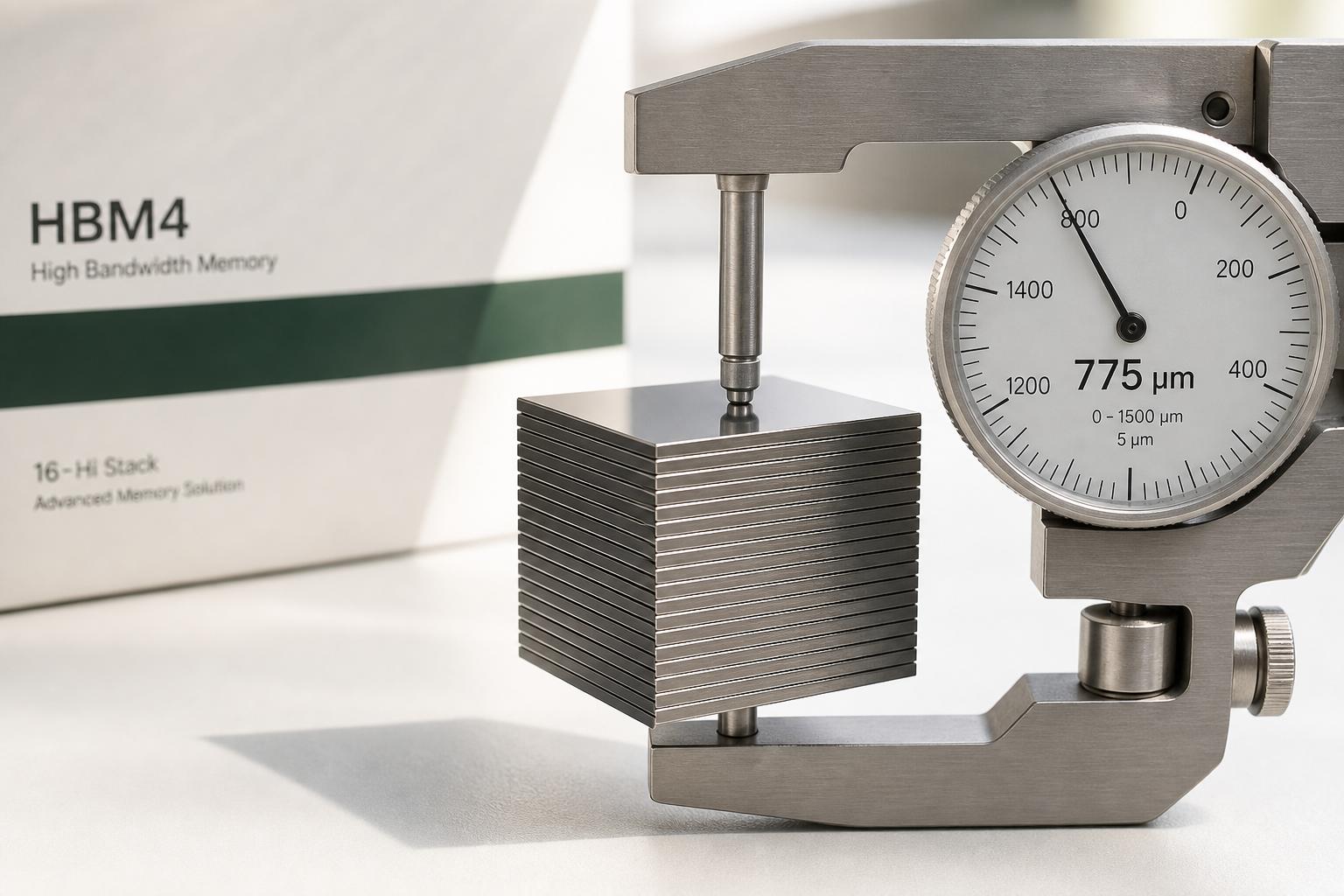
HBM4's strength is architectural headroom: a wider bus, more channels, higher stack density, and lower per-bit power. Those gains require a new HBM4-compatible controller, PHY, base logic die, and platform design rather than reuse of an HBM3 controller [1][11]. Semiengineering.com, drawing on Rambus's HBM controller IP business, argues that "no other memory architecture can practically deliver bandwidths of over 10 TB/s to a single GPU or accelerator" once several HBM4 stacks are combined around a processor die [10]. Its limitations are cost, yield, and manufacturing complexity. A DigiTimes-sourced report notes that HBM4 "requires a production cycle of four to six months alongside significantly lower initial yields" than mature HBM3E lines, and that HBM production overall "consumes roughly three times the wafer capacity of standard DDR5 DRAM," a structural constraint that keeps supply tight regardless of demand [22]. JEDEC's own height ceiling for the physical package, 775 micrometers (μm) for HBM4 at the time mass production began in early 2026, up from roughly 720 μm for HBM3E, is itself under active revision, with JEDEC "discussing easing the HBM product height to up to 900 micrometers" to make room for taller, higher-capacity stacks [23]. That packaging churn, plus the fact that NVIDIA reportedly changed its per-pin speed requirement mid-qualification, means HBM4's real-world specifications have shifted meaningfully even within its first year of mass production, a volatility HBM3E, three generations into its life cycle, no longer exhibits.
Feature Comparison
Table 1 below consolidates the specifications documented across JEDEC's published standard, the Siemens EDA design guide, and the three memory vendors' own product disclosures, isolating the parameters that most directly affect AI accelerator design: interface width, channel count, per-pin speed, bandwidth, capacity, voltage, and manufacturing status as of July 2026.
| Parameter | HBM3E | HBM4 |
|---|---|---|
| Interface width | 1,024-bit [1] | 2,048-bit, doubled [9] |
| Independent channels | 16 [9] | 32, with 2 pseudo-channels each [10] |
| Per-pin data rate | 9.2 to 12.4 Gb/s typical range [1] | 8 Gb/s JESD270-4-specified rate; over 11 Gb/s (Micron), over 10 Gb/s (SK hynix), 11.7 to 13 Gb/s (Samsung) in shipping product [15] [2] |
| Bandwidth per stack | Over 1.2 TB/s, up to 1.33 TB/s [1] | 2.048 TB/s at the JESD270-4-specified 8 Gb/s rate; higher figures are vendor-specific |
| Capacity per stack | Up to 36 GB (12-high) [1] | Up to 64 GB (16-high, 32Gb dies); 36 GB in first-wave 12-high parts [9] |
| Core / IO voltage | Roughly 1.1V core [1] | VDDQ 0.7 to 0.9V, VDDC 1.0 to 1.05V [9] |
| Power efficiency gain | 2.5x versus HBM2E [1] | 20% (Micron) to over 40% (SK hynix) versus HBM3E at equal capacity [14] [24] |
| Controller compatibility | Native | Requires an HBM4-capable controller and PHY [12] |
| Reliability feature | Standard refresh management | Directed Refresh Management (DRFM) for row-hammer mitigation [10] |
| Production status, July 2026 | In high-volume production, roughly two-thirds of 2026 HBM shipments | Ramping across SK hynix, Samsung, Micron; supply-constrained and pre-sold [22] |
The table shows that HBM4's advantage is not simply "faster HBM3E." The doubled interface and channel count change how many independent memory transactions an accelerator can issue in parallel, which matters disproportionately for inference workloads with irregular access patterns, while the lowered voltage rails reduce the power draw that increasingly limits how densely GPUs can be packed into liquid-cooled racks. The capacity row is the one counter-intuitive result: in first-wave 12-high parts, HBM4 does not yet exceed HBM3E's 36 GB ceiling per stack, so buyers expecting an automatic capacity jump alongside the bandwidth jump need to specifically confirm stack height and die density on the part they are quoted, since 16-high, 64 GB HBM4 remains a later-arriving configuration rather than the initial default.
Performance and Benchmarks
Independent, apples-to-apples third-party benchmarks comparing HBM3E and HBM4 accelerators are not yet public as of July 2026, since HBM4-based systems only entered volume shipment in the first quarter of the year; the performance figures available are vendor-published platform specifications and vendor-commissioned comparisons against the immediately prior generation, which this report treats as directional claims rather than independently verified results. With that caveat, the platform-level deltas are large and consistent across both major GPU vendors.
NVIDIA's own comparison places the Rubin GPU's HBM4 subsystem at "288 GB HBM4 | 22 TB/s" against the prior Blackwell generation's "192 GB HBM3e" at roughly 8 TB/s, a bandwidth increase tech-insider.org's independent analysis of NVIDIA's GTC 2026 disclosures describes as "nearly tripling Blackwell's 8 TB/s on HBM3e" [25]. At rack scale, NVIDIA states that "NVIDIA Vera Rubin NVL72 delivers up to 10x more tokens per megawatt than NVIDIA GB200 NVL72" [16], and separately claims the rack trains mixture-of-experts (MoE) models with one-fourth the number of GPUs compared to GB200 NVL72, and delivers AI inference at one-tenth the cost per million tokens versus Blackwell. Because these figures rest on NVIDIA-selected model configurations, principally the Kimi-K2-Thinking model at specific input and output sequence lengths per the footnotes on NVIDIA's own page, they should be read as best-case platform marketing claims pending independent reproduction, not as generalizable multipliers across all workloads.
AMD's competing claims follow the same pattern. Phoronix's coverage of AMD's own CES 2026 disclosures states the MI400-series flagship is "expected to have 432GB of HBM4 memory, 40 PFlops for FP4 and 20 PFlops of FP8, and 19.6TB/s of memory bandwidth" per GPU [18], and that the Helios rack built from 72 of those GPUs is "expected to achieve 1.4 PB/s of memory bandwidth, 43 TB/s of scale out bandwidth, 31 TB of HBM4 memory, and 2.9 ExaFLOPS of FP4 compute" [18]. An independent analysis on jaredwatkins.com contextualizes the memory figure directly against NVIDIA's prior generation, noting "the MI455X's 432 GB HBM4 per chip represents roughly 2.25x the memory of the NVIDIA B200 (192 GB)" [19], and flags that the same source's peak compute figures are "AMD stated, not independently verified" [19]. On the memory side specifically, the direct HBM4-versus-HBM3E delta that Micron itself publishes, 2.3 times the bandwidth of an equivalent-capacity HBM3E part with more than 20% better power efficiency, is the most conservative, apples-to-apples figure available, since it holds capacity constant and isolates the interface and process change [21].
Google's Ironwood (TPU7x) accelerator illustrates that HBM3E itself, deployed skillfully, still supports the largest current AI serving workloads: Google Cloud's own documentation lists "192 GB of HBM, with bandwidth of approximately 7.37 TB/s" per Ironwood chip [26], a figure achieved by pairing two 96 GB HBM chiplets, each "a self-contained unit with one TensorCore, two SparseCores, and 96 GB of high-bandwidth memory (HBM)" [26]. Ironwood's HBM bandwidth per chip is still below a single Rubin GPU's 22 TB/s, underscoring that raw per-chip HBM4 bandwidth is currently a NVIDIA-and-AMD-GPU-specific advantage rather than a universal AI-chip baseline; custom ASICs from Google, Amazon, and Meta have generally stayed on HBM3E through their current shipping generations even as their designers plan HBM4 for future iterations.
Data Analysis and Evidence
The quantitative case for HBM4 rests on four data sets: JEDEC's own specification numbers, vendor-published bandwidth and efficiency deltas, third-party market-size and market-share estimates, and pricing data. Table 2 below assembles the historical generation-over-generation bandwidth and capacity progression that underlies the entire HBM roadmap, drawn primarily from Wikipedia's aggregation of JEDEC and vendor disclosures, cross-checked against the vendor sources used elsewhere in this report.
| Generation | JEDEC announced / vendor introduced | Max data rate per pin | Interface width | Max bandwidth per stack |
|---|---|---|---|---|
| HBM3 | January 27, 2022 [3] | 6.4 Gb/s | 1,024-bit | 819.2 GB/s [3] |
| HBM3E | Vendor introductions from May 2023 | Up to 12.4 Gb/s [1] | 1,024-bit | Up to 1.33 TB/s [1] |
| HBM4 | April 16, 2025 (JESD270-4) [3] | 8 Gb/s baseline; over 13 Gb/s demonstrated by Samsung | 2,048-bit | Over 2.0 TB/s shipping [24] |
| HBM4E (announced) | Previewed March 2026 | 16 Gb/s | 2,048-bit | 4.0 TB/s [15] |
On market size, BofA's estimate of a $54.6 billion 2026 HBM market, a 58% year-over-year increase, is the headline figure SK hynix cites in its own investor communications, and Goldman Sachs separately forecasts that HBM demand for custom-ordered, ASIC-based AI chips will grow by 82%, accounting for one-third of the market [6]. Vendor concentration remains extreme: Counterpoint Research, in figures SK hynix's own investor materials cite, put the company at a 62% share of HBM shipments as of the second quarter of 2025 and 57% of revenue as of the third quarter, and Silicon Analysts' independent vendor tracker separately puts SK hynix's share at "50-55%" [8], a modest discrepancy between sources that reflects the difference between shipment-count share and revenue share as well as differing measurement dates.
TrendForce's demand-side analysis quantifies why HBM4 capacity per chip matters operationally: "HBM capacity per AI chip increasing significantly from 96GB/192GB to 216GB/288GB" in 2026, with NVIDIA's follow-on Rubin Ultra platform expected to push "HBM capacity per GPU to 384GB" in 2027 [27]. At the wafer level, TrendForce estimates HBM will consume "approximately 18%, 22%, and 30% of total DRAM wafer input" among top suppliers across 2025, 2026, and 2027 respectively, even though HBM bit supply remains a much smaller "approximately 8%, 9%, and 13%" share of total DRAM bit output over the same years, a gap that explains why HBM production is disproportionately squeezing conventional DRAM and DDR5 capacity [27]. Wikipedia's aggregation of 2026 commentary corroborates the spillover effect, noting that commodity DRAM and NAND flash pricing "experienced compounded increases, some exceeding 200%, since early 2025," and citing Micron's disclosure of "a 3-to-1 conversion ratio between HBM and DDR5 wafer capacity," meaning every unit of HBM ramped compresses roughly three units of general-purpose memory supply [3]. Interestingly, TrendForce's own 2Q26 research also finds that under current annual pricing mechanisms, "HBM wafer revenue was overtaken by DDR5 64GB RDIMM in 1Q26," a reminder that HBM's technical superiority has not automatically translated into superior near-term per-wafer profitability for suppliers, given how DDR5 prices spiked in the same period [27].
Pricing data show HBM4's cost premium clearly, though sources differ on magnitude. Silicon Analysts' July 2026 tracker lists HBM3 at roughly $200 per 24 GB stack, HBM3E at roughly $300 per 36 GB stack, and estimates HBM4 at roughly $500 per 48 GB stack, moving from $8.33 per GB for HBM3E to about $10.42 per GB for HBM4 [8]. At the GPU level, the same tracker attributes $2,400 of a NVIDIA B200's bill of materials to its eight HBM3E stacks alone, noting "HBM now represents 30-40% of total AI accelerator manufacturing cost, up from under 20% two generations ago" [8]. A community-sourced report discussed on Reddit, attributed to BusinessKorea, claims SK hynix's negotiated HBM4 supply price to NVIDIA settled at "around 560 dollars per product," describing that outcome as "more than 50% compared to its predecessor (HBM3E)" [28]. Forward-looking, DigiTimes-sourced reporting projects HBM4 could reach roughly $4 to $5 per gigabit or higher by 2027 as long-term agreements lock up supply, a figure this report notes should be treated as an industry-sourced projection rather than confirmed contract pricing [22]. Taken together, these figures show 40 to 70% cost premiums for HBM4 over HBM3E depending on the measurement point, a range consistent with SK hynix's own bandwidth and power-efficiency improvement figures of roughly double and 40%, respectively, suggesting the pricing largely reflects the performance delta rather than pure scarcity markup, though supply constraints described by TrendForce and DigiTimes are clearly amplifying the premium further.
Case Studies and Real-World Examples
NVIDIA Vera Rubin: The First HBM4-Native Flagship GPU Platform
NVIDIA's Vera Rubin platform is the clearest case of HBM4 being designed into a GPU architecture from the ground up rather than bolted onto an existing design. NVIDIA's product page states the Rubin GPU carries "288 GB HBM4 | 22 TB/s" of bandwidth, with the full Vera Rubin NVL72 rack aggregating "20.7 TB HBM4 | 1,580 TB/s" across 72 GPUs and 36 Vera CPUs [16]. GlobX's supply-chain analysis independently corroborates the chip-level figures, describing "the Rubin GPU" as packing "roughly 336 billion transistors, up to 288GB of next-generation HBM4 memory and around 22 TB/s of memory bandwidth" (Source: globx.eu). NVIDIA's own qualification process reportedly reshaped supplier behavior mid-cycle: EE Times reports NVIDIA "revised the HBM4 specifications for its Rubin GPUs in the third quarter of 2025, raising the required per-pin speed to above 11 Gbps," which forced "Micron, Samsung, and SK Hynix" to resubmit HBM4 samples against the new bar [2]. Micron confirmed it "has begun volume shipment of its HBM4 36GB 12H in the first quarter of calendar year 2026 and is designed for NVIDIA Vera Rubin," and described HBM4, in the words of its chief business officer, as the engine that delivers "unprecedented bandwidth, capacity and power efficiency" for next-generation AI platforms [21].
AMD Instinct MI400 and the Helios Rack: A Capacity-First HBM4 Strategy
Where NVIDIA's Rubin emphasizes per-GPU bandwidth, AMD's Instinct MI400 series is built around raw HBM4 capacity. Jaredwatkins.com's independent teardown notes the flagship MI455X ships with "432 GB HBM4; 19.6 TB/s bandwidth" per GPU, anchoring "AMD's Helios rack-scale system," described as "a double-wide rack housing 72 MI455X GPUs with 31 TB of HBM4 memory and a stated 2.9 exaFLOPS FP4 aggregate throughput" [19]. AMD's own newsroom confirms Helios is "powered by AMD Instinct MI455X accelerators, AMD EPYC Venice CPUs and AMD Pensando Vulcano NICs," delivering "up to 3 AI exaflops of performance in a single rack" [20], and the same release previews the 2027 MI500 series moving to "next-generation AMD CDNA 6 architecture, advanced 2nm process technology and cutting-edge HBM4E memory" [20]. GlobX frames the competitive stakes directly, noting industry reports "suggest it pushed NVIDIA to raise Rubin's memory bandwidth and power budget," positioning AMD's HBM4 capacity lead as a genuine architectural pressure point rather than a marketing footnote (Source: globx.eu).
SK hynix's World-First HBM4 Mass Production Milestone
SK hynix's September 2025 announcement remains the clearest single supplier milestone in the HBM4 timeline. The company said it had "completed development and prepared world-first mass production of HBM4, a next generation memory product for ultra-high performance AI," achieving "the industry's best data processing speed and power efficiency with the bandwidth doubled through adoption of 2,048 I/O terminals" [14]. Follow-on coverage at CES 2026 detailed the technical mechanism: SK hynix "utilized its proprietary Mass Reflow Molded Underfill (MR-MUF) technology to thin individual DRAM wafers to a staggering 30 µm to fit within JEDEC's strict 775-µm height limit," and paired with TSMC to use "12-nm logic as the base die" for its 16-layer HBM4 device, unveiled at CES 2026 as "a 16-layer HBM4 device with 48 gigabytes of capacity" [2]. SK hynix targets "the third quarter of 2026" for mass production of that 16-layer device [2].
OpenAI's Publicly Announced Hardware and Infrastructure Partnerships
OpenAI has publicly announced a collaboration with Broadcom to co-develop and deploy 10 gigawatts of OpenAI-designed AI accelerators, with deployments targeted to begin in the second half of 2026 and complete by the end of 2029 [29]. Separately, OpenAI, Samsung, and SK announced Stargate partnerships focused on expanding advanced-memory supply and Korean data-center capacity; the announcement says further scope and specifics will be shared as plans progress [30]. Neither public announcement identifies an HBM generation, an exclusive supplier, a supply quantity, a program codename, a contract value, or a claimed inference-cost reduction for OpenAI's custom accelerators. Those details should not be treated as confirmed HBM4 deployment evidence.
Implications and Future Directions
The near-term implication for buyers is straightforward: HBM3E remains the pragmatic choice through 2026 for any deployment prioritizing supply certainty and lower cost per gigabyte, while HBM4 is now the architecture NVIDIA's and AMD's flagship 2026 to 2027 platforms are built around, meaning any organization planning multi-year AI infrastructure procurement needs an HBM4 roadmap regardless of which vendor it standardizes on. TrendForce's forecast that HBM4 becomes "the market's mainstream project generation" for 2027 supply agreements signals that the transition window is narrow, roughly this single year, before HBM4 becomes the default rather than the premium option [27].
Packaging technology is the next visible constraint. Chosun's reporting on JEDEC's height-standard discussions notes that "hybrid bonding will be essential for 20-layer or higher HBM," according to SK hynix's own vice president of package development, and that Samsung has separately demonstrated hybrid copper bonding "achieving over 20% improvement in thermal resistance compared to TC bonding" [23]. Whether JEDEC ultimately relaxes the HBM height ceiling toward 900 μm will determine whether existing thermal-compression bonding equipment, on which Hanmi Semiconductor holds a reported "71.2%" share of the HBM bonder market, remains viable for another generation, or whether the industry pivots faster toward the hybrid-bonding equipment Hanwha Semiconductor and others are racing to commercialize [23]. That equipment decision, made largely by SK hynix, Samsung, and Micron rather than by GPU buyers, will materially affect HBM4E and later HBM4-generation pricing and availability through 2027 and 2028.
On capacity, the roadmap already extends beyond first-wave HBM4. Micron has demonstrated advanced packaging capability for stacking 16 dies of HBM by shipping HBM4 48GB 16H samples to customers, a configuration delivering "a 33% increase in capacity per HBM placement compared to the HBM4 36GB 12H offering" [21]. Samsung's HBM4E preview, targeting 16 Gb/s per pin and 4.0 TB/s bandwidth, effectively doubles current HBM4 bandwidth again within the same generational family, well before HBM5 standardization begins in earnest. For AI infrastructure planners, the practical guidance is to treat HBM4 not as a single fixed specification but as a moving target whose capacity, per-pin speed, and stack height will each be revised upward multiple times between 2026 and 2028, with NVIDIA's Rubin Ultra platform alone expected to lift per-GPU HBM capacity to 384 GB by 2027 [27].
Frequently Asked Questions (FAQs)
What is the main difference between HBM3E and HBM4? HBM4 doubles the physical memory interface from 1,024 bits to 2,048 bits and the channel count from 16 to 32, roughly doubling per-stack bandwidth from HBM3E's 1.2 to 1.33 TB/s range to a 2.048 TB/s JEDEC baseline, up to 3.3 TB/s in advanced configurations, while also lowering operating voltage for better power efficiency [1].
What are HBM4's key memory specs? JEDEC's JESD270-4 standard specifies a 2,048-bit interface, 32 independent channels, an 8 Gb/s baseline data rate yielding 2,048 GB/s per stack, stack heights up to 16-high with 32 Gb die density for a 64 GB capacity ceiling, VDDQ voltage options between 0.7V and 0.9V, and Directed Refresh Management for reliability [9] [10].
How does HBM3E bandwidth compare to HBM4? Micron specifies HBM3E bandwidth greater than 1.2 TB/s per placement. HBM4 provides 2.048 TB/s per stack at JESD270-4's specified 8 Gb/s data rate, while Micron rates its HBM4 product at more than 2.8 TB/s—a 2.3-times bandwidth improvement over an equal-capacity HBM3E stack according to Micron's generation-over-generation comparison [4] [11] [13].
When did HBM4 release? JEDEC finalized the HBM4 standard, JESD270-4, on April 16, 2025 [3], SK hynix announced world-first HBM4 mass-production readiness in September 2025, and Micron and Samsung both moved to high-volume production in the first quarter of calendar 2026, aligned with NVIDIA's Vera Rubin GTC 2026 launch in March [24].
Does HBM3E versus HBM4 make a meaningful difference in power consumption? Yes: Micron reports HBM4 delivers "over 20% better power efficiency compared to Micron's previous-generation HBM3E products" at equal capacity [24], while SK hynix reports its own HBM4 delivers more than 40% better power efficiency versus its prior generation, a difference the companies attribute to lower VDDQ and VDDC voltage rails specified in the JEDEC HBM4 standard.
Which NVIDIA GPU uses HBM4? NVIDIA's Vera Rubin platform, including the Rubin GPU and the Vera Rubin NVL72 rack, is NVIDIA's first HBM4-native architecture, specifying 288 GB of HBM4 and 22 TB/s of bandwidth per GPU [25]. NVIDIA's prior Blackwell generation, including the GB200 and B200, uses HBM3E [5].
How does HBM4 compare to HBM3E on capacity? In first-wave 12-high parts, capacity is unchanged at 36 GB per stack; Micron's own materials state HBM4 "12-high provides 36GB of memory capacity per stack (the same as the previous generation)" and that the generational advantage at that tier is purely bandwidth [13]. Capacity gains arrive with taller stacks: HBM4's 16-high configuration reaches a JEDEC-defined ceiling of 64 GB [9], and Micron's 48 GB 16-high samples already demonstrate meaningfully higher capacity per HBM placement than the 36 GB 12-high part.
What is a 12-hi HBM4 stack? "12-hi" (or 12-high) describes a stack of twelve individual DRAM dies bonded vertically on top of a base logic die and connected by through-silicon vias; it is the current mainstream HBM4 configuration, used by Micron's 36 GB shipping parts and SK hynix's initial HBM4 products, ahead of 16-high stacks that raise capacity further [23].
What does the high bandwidth memory roadmap look like through 2026 and beyond? 2026 is a transition year in which HBM3E still supplies roughly two-thirds of total HBM shipments while HBM4 ramps across all three qualified suppliers for NVIDIA's Vera Rubin and AMD's Instinct MI400 platforms; TrendForce expects HBM4 to become the market's mainstream generation for 2027 supply agreements [27], with HBM4E, targeting 16 Gb/s pin speeds and 4.0 TB/s per stack, already previewed for the following step.
Conclusion
The move from HBM3E to HBM4 is a genuine architectural transition, not an incremental speed bump. Doubling the memory interface to 2,048 bits, doubling the channel count to 32, and adding a lower-voltage power delivery scheme move from Micron HBM3E bandwidth greater than 1.2 TB/s per placement to a 2.048 TB/s JEDEC HBM4 baseline and more than 2.8 TB/s in Micron HBM4 parts, while suppliers report improved power efficiency [4] [11] [13]. Capacity gains, by contrast, arrive on a different timeline: first-wave 12-high HBM4 holds at the same 36 GB ceiling as HBM3E, with the real capacity jump, to 48 GB and eventually 64 GB, tied to 16-high stacks that remain earlier in their qualification cycle.
For buyers evaluating AI accelerators today, the practical decision hinges on timing and platform. HBM3E remains the safer, better-supplied, lower-cost choice, and it is used by products including NVIDIA's H200 and Blackwell fleet and AMD's MI350 series. AMD's MI300X uses HBM3. HBM4 is the memory NVIDIA's Vera Rubin and AMD's Instinct MI400 platforms are purpose-built around [31] [32]. OpenAI has separately announced custom-accelerator work with Broadcom and Stargate partnerships with Samsung and SK to expand advanced-memory supply, but it has not publicly confirmed an HBM4 capacity commitment for its custom silicon. With TrendForce projecting HBM4 will become the industry's mainstream supply generation for 2027 and pricing already tracking 40 to 70% above HBM3E by various measures, organizations planning AI infrastructure spend beyond the current calendar year should treat an HBM4 roadmap, and the supply commitments it requires well in advance of deployment, as a near-term procurement decision rather than a future one.
External Sources (32)
About
GPUSmith
Plan and build private AI compute with GPU Smith. We connect workload requirements with GPU hardware, networking, deployment and operating decisions so your infrastructure fits the work it must perform.
GPU Smith provides independent engineering and research for private AI infrastructure. We help technical buyers and operators reason about GPU workload sizing, hardware selection, procurement, deployment and inference operations, from the compute system to the networking, power and cooling requirements around it.
Start with the workload
Useful infrastructure decisions begin with the models, data, throughput, latency and operating constraints a team actually has. GPU Smith helps connect those requirements with system design and deployment choices. The goal is a privately controlled AI environment whose capacity and operational demands are understood before a purchasing decision.
Hardware and supplier research
Our public reference library covers GPUs, complete systems and networking components. The server-vendor directory and manufacturing research help teams investigate suppliers, compare options and follow sources behind technical claims. We distinguish manufacturer specifications from measured benchmarks and advertised capabilities from tested configurations. Reference pages are research resources, not a live inventory listing or a binding equipment quote.
Deployment and operations
GPU Smith's engineering scope includes infrastructure integration, networking, power, cooling and the practical operation of inference workloads. Our published articles explain the tradeoffs behind deployment, procurement and ongoing operations so teams can ask better questions and document decisions.
Work with GPU Smith
Explore the hardware library, GPU references, networking references and vendor research. Contact GPU Smith with your workloads and deployment constraints to discuss a project and confirm current scope, pricing and availability.
Inclusion of a manufacturer or product in our research does not imply a partnership, certification or endorsement.
Disclaimer
This document is provided for informational purposes only. No representations or warranties are made regarding the accuracy, completeness, or reliability of its contents. Any use of this information is at your own risk. GPUSmith shall not be liable for any damages arising from the use of this document. This content was generated with assistance from artificial intelligence tools, which may contain errors or inaccuracies. Readers should verify critical information independently. All product names, trademarks, and registered trademarks mentioned are property of their respective owners and are used for identification purposes only. Use of these names does not imply endorsement. This document does not constitute professional or legal advice. For specific guidance related to your needs, please consult qualified professionals.