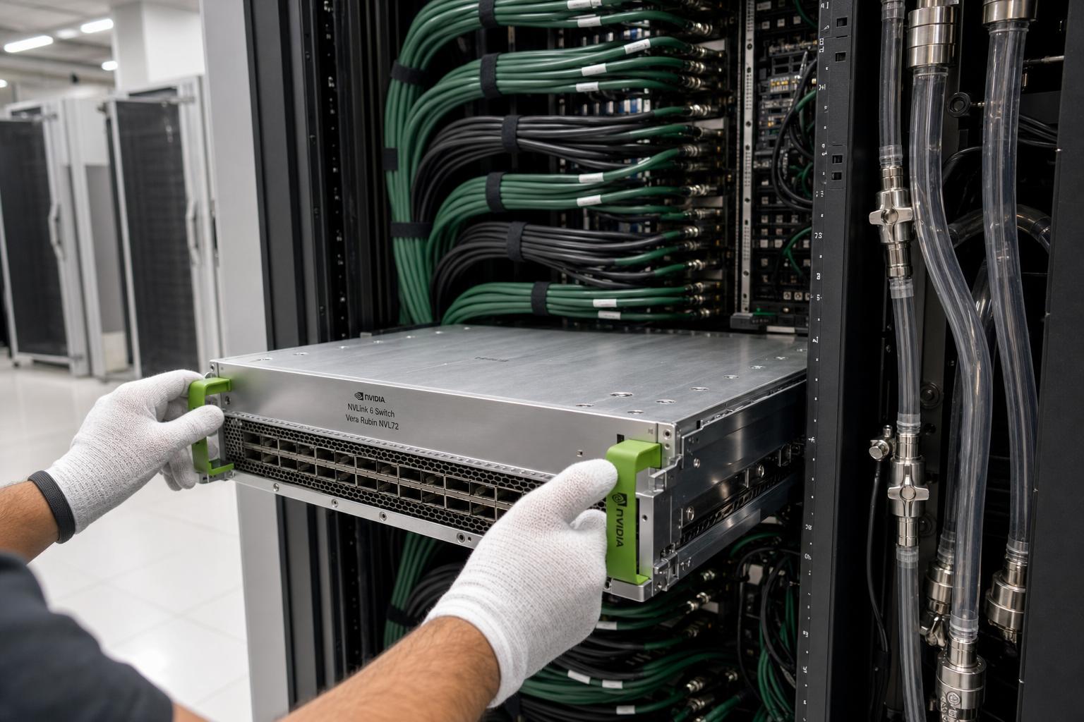
GPUSmith Article
NVLink 5 vs NVLink 6: Bandwidth, Domains and Cluster Design
Summary
- 01NVLink 6 doubles NVLink 5's per-GPU bandwidth from 1.8 TB/s to 3.6 TB/s while keeping the scale-up domain at 72 GPUs in both the GB200/GB300 and Vera Rubin NVL72 racks.
- 02As of July 2026, NVLink 5 is the field-proven, widely deployed standard, with GB200 NVL72 available at scale since 2025, while NVLink 6 is only entering full production and its performance claims still rest on NVIDIA's own simulations rather than independent benchmarks.
- 03The bigger structural leap was NVLink 4 to NVLink 5, which expanded the scale-up domain from 8 GPUs to 72 GPUs; NVLink 5 to NVLink 6 is primarily a bandwidth, latency and resiliency upgrade within that same 72-GPU topology.
- 04NVLink remains a scale-up, intra-rack technology, not a replacement for scale-out fabrics like Quantum-X800 InfiniBand at 800 Gb/s per port, which connect many NVLink domains into much larger clusters.
- 05NVIDIA's own simulated benchmarks claim NVLink 6 delivers up to 2.3x the decode throughput of off-the-shelf Ethernet in the same 72-GPU domain, but independent, third-party validation of Rubin-class hardware does not yet exist as of mid-2026.
Inside this article
- 01NVLink 5 vs NVLink 6: Bandwidth, Domains and Cluster Design
- 02Executive Summary
- 03Introduction and Background
- 04NVLink 5: Capabilities, Adoption, Strengths and Limitations
- 05NVLink 6: Capabilities, Adoption, Strengths and Limitations
- 06Feature Comparison
- 07Performance and Benchmarks
- 08NVLink vs InfiniBand and Scale-Out Networking
- 09Data Analysis and Evidence
- 10Case Studies and Real-World Examples
- 11Implications and Future Directions
- 12Frequently Asked Questions (FAQs)
- 13Conclusion
NVLink 5 vs NVLink 6: Bandwidth, Domains and Cluster Design
Executive Summary
NVIDIA's scale-up GPU interconnect jumped from NVLink 5 to NVLink 6 as the company transitioned its data center roadmap from the Blackwell architecture to the Rubin architecture. NVLink 5, shipping since 2024 in the B200, GB200 NVL72, and GB300 NVL72 platforms, delivers 1,800 GB/s (1.8 TB/s) of bidirectional bandwidth per GPU across 18 links, each running at 100 GB/s [1]. NVLink 6, introduced alongside the Rubin platform at CES 2026 and entering full production in mid-2026, doubles that figure to 3,600 GB/s (3.6 TB/s) per GPU over 36 links [2]. At the rack level, the flagship GB200 NVL72 and GB300 NVL72 systems connect 72 Blackwell-family GPUs into a single non-blocking NVLink domain with 130 TB/s of aggregate switch bandwidth [3], while the Vera Rubin NVL72 rack, ramping into full production as of July 2026, doubles that to 260 TB/s across the same 72-GPU topology [4] [5].
The generational gap is not just a bandwidth doubling. NVIDIA states NVLink 6 delivers up to 2.3x higher decode throughput on large mixture-of-experts (MoE) models compared with off-the-shelf Ethernet in the same 72-GPU domain, and it adds resiliency features including hot-swappable switch trays, control-plane resilience, and support for partially populated racks [6]. Independent researchers who benchmarked earlier NVLink generations have documented that GPU interconnect topology, not just headline bandwidth, materially affects real-world application performance, a caution that still applies to vendor-reported Rubin figures today [7].
Scale-up domain size, the number of GPUs that can talk to each other at full NVLink bandwidth without leaving the switch fabric, has stayed fixed at 72 GPUs across both the GB200/GB300 (NVLink 5) and Vera Rubin NVL72 (NVLink 6) racks, up from 8 GPUs in the Hopper-era NVLink 4 generation [8] [1]. Beyond the rack, NVLink remains a scale-up (intra-domain) technology, distinct from scale-out fabrics like NVIDIA Quantum-X800 InfiniBand, which delivers 800 Gb/s per port for connecting thousands of racks together [9].
Commercially, this transition is unfolding against record NVIDIA data center revenue of $75.2 billion in the first quarter of fiscal 2027 (the quarter ended April 26, 2026), up 92% year over year, with networking revenue alone reaching $14.8 billion, up 199% year over year [10]. Cloud providers including CoreWeave, Microsoft, and xAI have already deployed GB200 and GB300 NVL72 racks running NVLink 5 at scale, and NVIDIA has stated that Rubin-based, NVLink 6 systems are shipping to eight named hyperscale partners in the second half of 2026 [5]. For buyers evaluating cluster design today, the practical answer to "NVLink 5 vs NVLink 6" is that NVLink 5 is the shipping, field-proven standard underpinning most currently deployed trillion-parameter training and inference fleets, while NVLink 6 is the higher-bandwidth, higher-resiliency successor arriving with Rubin hardware that is only beginning to reach production racks as of mid-2026.
Introduction and Background
NVLink is NVIDIA's proprietary, point-to-point serial interconnect for GPU-to-GPU and, via NVLink-C2C, CPU-to-GPU communication. First announced in March 2014 and introduced commercially in 2016 with the Pascal-based Tesla P100, NVLink was designed to overcome the bandwidth ceiling of PCI Express (PCIe) for multi-GPU systems [11]. The original NVLink 1.0 delivered 160 GB/s of bidirectional bandwidth per GPU across four links, roughly five times the bandwidth of a PCIe 3.0 x16 slot at the time [8]. Hot Chips presentations from NVIDIA's own systems architects corroborate this trajectory, showing 40 GB/s per link and 160 GB/s total for the 2016 P100-based NVLink 1 generation [12]. By comparison, a single PCIe Gen4 x16 slot delivers only about 32 GB/s unidirectional, and even PCIe Gen5 x16 tops out at roughly 64 GB/s bidirectional, making current-generation NVLink 5 alone on the order of 55 times faster than the PCIe fallback most workstation-class GPUs still rely on [13].
Each subsequent NVIDIA GPU architecture has paired with a new NVLink generation: NVLink 2.0 with Volta (V100, 300 GB/s), NVLink 3.0 with Ampere (A100, 600 GB/s), NVLink 4.0 with Hopper (H100, 900 GB/s), and NVLink 5.0 with Blackwell (B100/B200/GB200, 1.8 TB/s) [13]. The transition from a purely point-to-point mesh to a switched fabric came in 2018 with the introduction of NVSwitch, first deployed in the V100-based DGX-2 system, which enabled full interconnectivity among 16 GPUs in a single chassis rather than the smaller, partial mesh possible with direct GPU-to-GPU links alone [8]. By the Hopper generation, NVIDIA's own conference materials show DGX H100 SuperPODs achieving 3.6 TB/s of bisection bandwidth and 450 GB/s of AllReduce bandwidth, versus 140 GB/s and 40 GB/s respectively for the original 2016 DGX-1 [12].
This distinction between scale-up and scale-out networking is central to understanding why NVLink exists alongside InfiniBand and Ethernet rather than replacing them. Scale-up fabrics connect the GPUs inside a single coherence domain, typically a rack, with the highest possible bandwidth and lowest possible latency, so that dozens of GPUs can behave as one giant accelerator with pooled high-bandwidth memory (HBM). With NVLink Switch, individual NVLink connections can be extended across nodes to create a seamless, high-bandwidth, multi-node GPU cluster that NVIDIA describes as effectively forming a data-center-sized GPU[1]. A specialized implementation called Multi-Node NVLink (MNNVL) "extends the NVLink fabric across multiple chassis, presenting up to 72 GPUs as a single NVLink domain," the same mechanism that lets an entire rack, not an individual server, function as the base unit of compute [13]. Scale-out fabrics such as InfiniBand and Ethernet then connect many of those domains together across a data center, prioritizing reach and aggregate cluster size over the ultra-low latency needed inside a domain.
The stakes of this comparison have risen sharply because large language model (LLM) training and, increasingly, inference now depend on parallelism strategies (tensor parallelism, expert parallelism, pipeline parallelism) that require constant, high-volume communication between GPUs. Independent academic benchmarking of earlier NVLink and NVSwitch generations found several communication-network non-uniform memory access (NUMA) effects tied to link topology and routing, underscoring that a GPU's position within an interconnect fabric, not only its raw link count, materially affects delivered performance [7]. That is part of the underlying reason NVIDIA has pushed NVLink bandwidth up so aggressively, doubling it with nearly every architecture generation while also expanding the domain size from 8 GPUs in Hopper-era DGX systems to 72 GPUs in the Blackwell and Rubin NVL72 racks, a nine-fold increase in scale-up domain size in roughly two years.
This report compares NVLink 5 and NVLink 6 in detail: their raw bandwidth and topology, the platforms each ships in, how they compare to InfiniBand and Ethernet scale-out fabrics, and what the transition means for organizations planning GPU cluster purchases or cloud capacity commitments as of July 2026.
NVLink 5: Capabilities, Adoption, Strengths and Limitations
Capabilities
NVLink 5 is the interconnect generation paired with NVIDIA's Blackwell GPU architecture, covering the B100, B200, B200A, and Blackwell Ultra (B300) data center GPUs. Each Blackwell GPU supports up to 18 NVLink 5 connections, each running at 100 GB/s bidirectionally, for a total of 1,800 GB/s (1.8 TB/s) of bidirectional bandwidth per GPU, roughly double the 900 GB/s of NVLink 4 on Hopper and over 14 times the bandwidth of a PCIe Gen5 x16 slot [14]. NVIDIA rates a single Blackwell Tensor Core GPU at up to 18 NVLink 100 gigabyte-per-second connections, matching that same 1.8 TB/s total [1].
At the switch level, each NVLink 5 Switch application-specific integrated circuit (ASIC) provides 72 ports at 400 Gb/s each, and each B200 GPU connects to two NVSwitch chips using 9 NVLink connections apiece (9+9=18 total) [2] [8]. The flagship rack-scale implementation is the GB200 NVL72, which connects 36 Grace CPUs and 72 Blackwell GPUs via nine NVLink Switch trays (18 NVSwitch ASICs total) into a single, non-blocking, all-to-all NVLink domain, delivering 130 TB/s of aggregate GPU communication bandwidth [3]. NVIDIA describes this rack as functioning like "one massive GPU," with each B200 GPU inside the NVL72 domain able to reach any of the other 71 GPUs at the full 1.8 TB/s NVLink rate [14]. Operating that domain reliably has its own software prerequisites: multi-node NVLink support requires NCCL 2.25.2 or later, and the NVIDIA IMEX service must be running and correctly configured on every node in the domain before cross-node NVLink memory access will function at all [14].
Blackwell Ultra's GB300 NVL72 uses the same fifth-generation NVLink fabric, providing an identical 130 TB/s of aggregate bandwidth per rack, but pairs it with 1.5x more dense FP4 compute and roughly 21 TB of HBM3e memory per rack, a 1.5x increase over GB200 NVL72's HBM capacity [15]. Outside the rack, GB200 and GB300 systems scale out over NVIDIA Quantum-X800 InfiniBand or Spectrum-X Ethernet, using ConnectX-8 SuperNICs, to link many NVL72 racks into larger clusters [3].
Adoption
NVLink 5 was announced with Blackwell in 2024, and GB200 NVL72 systems became available to customers at scale in 2025. CoreWeave announced general availability of GB200 NVL72 rack-scale systems, initially serving customers Cohere, IBM, and Mistral AI, and stated its instances are scalable up to 110,000 Blackwell GPUs with NVIDIA Quantum-2 InfiniBand networking [16]. CoreWeave also reported a new industry record in AI inference with NVIDIA GB200 Grace Blackwell Superchips in the MLPerf v5.0 benchmark suite, an industry-standard measure of machine learning performance across realistic deployment scenarios [16]. A separate GB200 NVL72 demonstration, connecting 36 Grace CPUs and 72 Blackwell GPUs with Quantum-2 InfiniBand at 400 Gb/s of bandwidth per GPU, delivered up to 1.4 exaFLOPS of AI compute [17].
Microsoft built its Fairwater AI datacenter campus in Wisconsin, spanning 315 acres and 1.2 million square feet, around GB200 NVL72 racks, describing the site as running "a single, massive cluster of interconnected NVIDIA GB200 servers" and claiming it will deliver 10 times the performance of the world's fastest supercomputer at the time of writing [18]. Microsoft has since connected multiple Fairwater sites, including a second campus in Atlanta, into what it calls an "AI superfactory," a distributed network built to "act as a virtual supercomputer" running one complex job across millions of pieces of hardware rather than a single site training a model in isolation [19]. Atlanta's Fairwater site likewise uses NVIDIA GB200 NVL72 rack-scale systems that Microsoft states "can scale to hundreds of thousands of NVIDIA Blackwell GPUs" [19].
xAI's Colossus facility in Memphis had, as of late 2025, roughly 200,000 H100/H200 GPUs plus approximately 30,000 GB200 NVL72 GPUs operating as what independent analysts describe as "the largest fully operational, single-coherent cluster" outside multi-datacenter training approaches [20]. By January 2026, xAI had purchased a third building near Colossus 2, bringing total site capacity to roughly 2 gigawatts and 555,000-plus GPUs, a purchase reportedly valued at approximately $18 billion [21]. CoreWeave later became the first provider to bring up the successor GB300 NVL72 platform in collaboration with Dell Technologies and Switch, in what it called an "industry first" bring-up [22].
Strengths and Limitations
NVLink 5's strengths are maturity, a proven software stack (NCCL, NIXL, TensorRT-LLM, and Dynamo all ship tuned for it), and wide availability across every major hyperscaler and neocloud as of mid-2026. Its principal limitation, addressed directly by NVLink 6, is bandwidth headroom: as MoE models and long-context reasoning workloads push more tokens through GPU-to-GPU links, 1.8 TB/s per GPU becomes a tighter ceiling relative to compute growth. NVLink 5 racks also lack several of the resiliency features introduced in NVLink 6, discussed in detail below, such as hot-swappable switch trays and dynamic traffic rerouting around failed links, meaning maintenance on an NVLink 5 rack is comparatively more likely to require partial or full rack downtime. A further limitation is topology rigidity: multi-GPU communication in NVLink Switch systems is only uniform within a single 72-GPU domain, and crossing that boundary without topology-aware job scheduling produces a documented bandwidth cliff from roughly 800-plus GB/s down to 100 to 200 GB/s, which is why infrastructure guides describe Slurm's topology and block plugins, combined with per-job IMEX isolation, as "non negotiable on production clusters" once multiple racks are combined into a single training job [14]. Some of these operational pitfalls, tied to verifying fabric health and correctly configuring NCCL and IMEX, are described by infrastructure engineers as having "burned early adopters in 2025" during the initial Blackwell ramp [14].
- 01Upgrade NCCL
Multi-node NVLink (MNNVL) support requires NCCL 2.25.2 or later before cross-node communication can be enabled.
- 02Configure IMEX
The NVIDIA IMEX service must be running and correctly configured on every node in the domain before cross-node NVLink memory access will function at all.
- 03Apply topology-aware scheduling
Slurm's topology and block plugins, combined with per-job IMEX isolation, are treated as non negotiable once multiple racks are combined into a single training job.
Cross-node NVLink memory access works correctly and jobs stay within the full-bandwidth 72-GPU domain.
Crossing an NVLink domain boundary without topology-aware scheduling produces a bandwidth cliff from roughly 800-plus GB/s down to 100 to 200 GB/s.
NVLink 5 is the shipping, field-proven standard underpinning most currently deployed trillion-parameter training and inference fleets, while NVLink 6 is the higher-bandwidth, higher-resiliency successor arriving with Rubin hardware that is only beginning to reach production racks as of mid-2026.
NVLink 6: Capabilities, Adoption, Strengths and Limitations
Capabilities
NVLink 6 is the interconnect generation introduced with NVIDIA's Rubin platform, unveiled in detail at CES 2026. Each Rubin GPU supports 36 NVLink 6 connections, twice the link count of NVLink 5, for a total of 3,600 GB/s (3.6 TB/s) of bidirectional bandwidth per GPU, twice the previous generation's 1.8 TB/s [23]. NVLink 6 Switch ASICs retain the same 72-port count as NVLink 5 switches but run at double the per-port rate, with each switch tray in a Vera Rubin rack containing four NVLink ASICs. Independent hardware trackers add that each Rubin GPU also carries up to 20.5 TB/s of its own on-package HBM4 bandwidth, separate from the 3.6 TB/s of NVLink 6 bandwidth used to reach other GPUs in the rack [24].
The flagship implementation is the Vera Rubin NVL72 rack, unifying 72 Rubin GPUs and 36 Vera CPUs, which delivers 3.6 TB/s per-GPU bandwidth and 260 TB/s of aggregate rack-level GPU-to-GPU bandwidth, twice the 130 TB/s of GB200/GB300 NVL72 [5]. In total, a single Vera Rubin NVL72 rack contains 20.7 TB of pooled HBM4 memory running at 1,580 TB/s of aggregate bandwidth [4]. At the collective-compute level, the full rack provides 130 TFLOPS of FP8 in-network compute for accelerating reductions and other collective operations, with each individual switch tray contributing 28.8 TB/s of tray-level bandwidth and 14.4 TFLOPS of that total [6]. The sixth-generation NVLink Switch also introduces new management and resiliency features designed to maximize system uptime, including control plane resilience, operation with a partially populated rack, and hot-swapping of switch trays [23].
Smaller NVLink 6 configurations also exist. The DGX Rubin NVL8 server, an eight-GPU node, delivers 176 TB/s of aggregate GPU memory bandwidth and uses NVLink 6 with 28.8 TB/s of total switch bandwidth within the node [25]. Networking beyond the rack uses ConnectX-9 SuperNICs, which deliver 1.6 Tb/s of scale-out bandwidth per GPU, twice the 800 Gb/s of the ConnectX SuperNIC generation used with GB300 NVL72 [5]. Vera CPUs connect to Rubin GPUs over NVLink-C2C at 1.8 TB/s of coherent bandwidth, seven times the bandwidth of PCIe Gen6 [5].
Adoption
Vera Rubin entered full production on approximately June 1, 2026, with Jensen Huang announcing the milestone at GTC Taipei; partner shipments to eight named cloud providers, including AWS, Google Cloud, Microsoft, Oracle Cloud Infrastructure (OCI), and CoreWeave, were expected to begin in the second half of 2026 [26]. Independent trade coverage confirms the standalone Rubin GPU is built on a TSMC N3-class process with 336 billion transistors, up from Blackwell's 208 billion on B200, and that Rubin "talks to its neighbors over sixth-generation NVLink at 3.6 TB/s per GPU, a step up from NVLink 5's role in Blackwell-generation racks" [26]. CoreWeave has already published projections of a 10x improvement in tokens per megawatt for Vera Rubin NVL72 relative to Blackwell-based systems, positioning itself among the earliest cloud partners for the transition [4]. As of July 2026, however, adoption remains in its earliest stages relative to NVLink 5, whose GB200 NVL72 systems had been available to customers at scale since 2025.
Strengths and Limitations
NVLink 6's core strength is delivered bandwidth combined with new operational discipline. NVIDIA states that in simulated large-scale MoE inference workloads (DeepSeek-R1, Qwen 235B, and a 2 trillion-parameter model), NVLink 6 in a 72-GPU domain delivers up to 2.3x the decode throughput of leading off-the-shelf Ethernet at comparable interactivity targets [6]. The sixth generation switch also supports software-defined routing with management-controller fallback, dynamic traffic rerouting, in-service software updates, and fine-grained link telemetry for monitoring and fault attribution, on top of the control-plane resilience and hot-swap capability introduced with the platform. The clearest limitation, as of mid-2026, is production maturity: independent trackers note that "no independent benchmarks exist yet" for Rubin-class systems and that "all performance figures are NVIDIA-sourced projections," a caveat that will only resolve once third-party MLPerf submissions and customer deployments accumulate through late 2026 and into 2027 [24]. Pricing has not been officially disclosed either; one industry estimate notes the predecessor GB200 NVL72 "was reportedly in the $2-3M range," with NVL144-class Rubin racks expected to cost more [24].
It is also worth flagging a naming discrepancy that has caused confusion in early Rubin coverage. Some outlets and NVIDIA's own pre-launch materials referred to the platform as "VR200 NVL144," counting each of the two GPU dies inside a Rubin Superchip package separately for a total of 144 dies, while NVIDIA's shipping product pages describe the same rack as "Vera Rubin NVL72," counting 72 integrated GPU packages [27]. Industry trade press has explicitly documented the reversal, noting that "early in development the rack was informally called 'NVL144,' a die-count label," but that "Nvidia reverted to 'NVL72' to count physical GPU packages instead, matching the convention it used for GB200 and GB300" [26]. This mirrors the same package-versus-die counting convention NVIDIA used for GB200, where each superchip likewise integrates two Blackwell dies but is counted as one logical GPU [28].
- 1,800 GB/s (1.8 TB/s) per-GPU bandwidth across 18 links
- 130 TB/s aggregate bandwidth across the 72-GPU GB200/GB300 NVL72 domain
- Mature software stack and wide availability across every major hyperscaler and neocloud as of mid-2026
- GB200 NVL72 systems became available to customers at scale in 2025
- 3,600 GB/s (3.6 TB/s) per-GPU bandwidth across 36 links
- 260 TB/s aggregate bandwidth across the 72-GPU Vera Rubin NVL72 domain
- Up to 2.3x higher decode throughput than off-the-shelf Ethernet in simulated MoE workloads
- No independent benchmarks exist yet; all performance figures are NVIDIA-sourced projections
NVLink 6 figures are NVIDIA-sourced simulations, independent MLPerf validation is expected only later in 2026 and into 2027.
Feature Comparison
NVLink 1.0 launched in 2016 with the Pascal-based Tesla P100, delivering 160 GB/s of bidirectional bandwidth per GPU.
NVLink 2.0 arrived with the Volta-based V100, lifting per-GPU bandwidth to 300 GB/s.
NVLink 3.0 shipped with the Ampere-based A100, doubling bandwidth again to 600 GB/s.
NVLink 4.0 paired with the Hopper-based H100, reaching 900 GB/s of per-GPU bandwidth.
NVLink 5.0 arrived with Blackwell (B100/B200/GB200), doubling bandwidth to 1,800 GB/s per GPU.
NVLink 6 launched with the Rubin platform, doubling bandwidth again to 3,600 GB/s per GPU.
Table 1 below consolidates the headline specifications for the fourth, fifth, and sixth NVLink generations, cross-checked against NVIDIA's own specifications page and multiple independent technical sources. Because all three generations remain commercially relevant (Hopper-based fleets are still widely deployed, Blackwell is the current production standard, and Rubin is entering production), the fourth-generation column is retained for context.
| Specification | NVLink 4 (Hopper) | NVLink 5 (Blackwell) | NVLink 6 (Rubin) |
|---|---|---|---|
| Per-GPU bandwidth | 900 GB/s [11] | 1,800 GB/s [13] | 3,600 GB/s [2] |
| Max links per GPU | 18 (see Per-GPU bandwidth row) | 18 (see Per-GPU bandwidth row) | 36 (see Per-GPU bandwidth row) |
| Per-link speed | 25 GB/s per direction (50 GT/s) [11] | 50 GB/s per direction (100 GT/s) [11] | 50 GB/s per direction (400 Gb/s), or 100 GB/s bidirectional per link |
| Switch GPU domain size | 8 GPUs (see below) | 8 or 72 GPUs (see below) | 8 or 72 GPUs [23] |
| Aggregate rack bandwidth (NVL72) | 7.2 TB/s (8-GPU baseline) | 130 TB/s (see NVLink 5 Capabilities above) | 260 TB/s (see NVLink 6 Capabilities above) |
| In-network compute (FP8, full rack) | Not published at NVL72 scale | Approximately 65 TFLOPS (derived) | 130 TFLOPS (see NVLink 6 Capabilities above) |
| Flagship platform | DGX H100 / HGX H100 [12] | GB200 NVL72 / GB300 NVL72 | Vera Rubin NVL72 |
| CPU-GPU coherent link (NVLink-C2C) | 900 GB/s (Grace Hopper) [11] | Not separately published at GB200 scale | 1.8 TB/s (see NVLink 6 Capabilities above) |
| Resiliency features | Standard | Standard | Hot-swap trays, control plane resilience, partial-rack operation (see NVLink 6 Capabilities above) |
| Production status (as of July 2026) | Widely deployed since 2022 | Widely deployed since 2025 | Entering production mid-2026 [26] |
Table 1 shows that the raw per-GPU bandwidth doubled with each generational jump (900 to 1,800 to 3,600 GB/s), a pattern NVIDIA has sustained on roughly a two-year cadence since Hopper. The more consequential shift for buyers evaluating whole-system performance, however, is the change from 8-GPU to 72-GPU switch domains that occurred between NVLink 4 and NVLink 5; NVLink 6 preserved that 72-GPU domain size while doubling both the per-link speed and the in-network compute available to accelerate collective operations. In practice this means an organization moving from an NVLink 4 (Hopper) fleet to an NVLink 5 (Blackwell) fleet experiences a much larger structural change (from 8-GPU to 72-GPU coherence domains) than one moving from NVLink 5 to NVLink 6, which is primarily a bandwidth, latency, and resiliency upgrade within the same domain topology.
Performance and Benchmarks
Independent, peer-reviewed benchmarking of GPU interconnects has historically lagged vendor announcements by several years. The most cited academic evaluation, published in IEEE Transactions on Parallel and Distributed Systems and available as a preprint, conducted "a thorough evaluation on five latest types of modern GPU interconnects: PCIe, NVLink-V1, NVLink-V2, NVLink-SLI and NVSwitch" across DGX-1, DGX-2, and Summit-class systems, identifying several NUMA effects specific to NVLink's topology, connectivity, and routing that are not visible from bandwidth specifications alone [7]. No equivalent independent, peer-reviewed study of NVLink 5 or NVLink 6 has yet been published as of July 2026; the performance figures available for these generations come from NVIDIA itself or from cloud providers running NVIDIA-designed benchmark suites such as MLPerf.
On NVLink 4 era hardware, NVIDIA's own historical documentation of the NVSwitch architecture, presented at Hot Chips, reported a 900 GB/s per-GPU aggregate bandwidth and, at DGX H100 SuperPOD scale, a 57.6 TB/s bisection bandwidth across the full scalable unit with 450 GB/s of AllReduce bandwidth [12]. The same NVIDIA architecture materials trace this bisection-bandwidth growth across every DGX generation between the original 2016 DGX-1 and the 2022 DGX H100, moving through 2.4 TB/s of bisection bandwidth and 75 GB/s of AllReduce bandwidth on the 2018 DGX-2 along the way [12]. For NVLink 5, NVIDIA's GB200 NVL72 materials claim 30x faster real-time trillion-parameter LLM inference and 4x faster large-scale training versus an H100-based cluster of the same size scaled over InfiniBand, based on a cluster size of 32,768 GPUs comparing 4,096 HGX H100 nodes against 456 GB200 NVL72 nodes [3]. CoreWeave, running its own MLPerf Inference v5.0 submission on GB200-based instances, reported 2.86x better per-GPU inference performance compared with its H100-based instances, an independently submitted (though vendor-affiliated) data point that corroborates the scale of improvement NVIDIA claims for the Hopper-to-Blackwell, NVLink 4-to-5 transition [15].
For NVLink 6, NVIDIA's own simulation-based figures show 2.3x higher decode throughput than off-the-shelf Ethernet on a Qwen 235B model at 120 tokens/second/user interactivity, 2.1x on DeepSeek-R1 at 300 tokens/second/user, and 2.0x on a simulated 2 trillion-parameter model at 80 tokens/second/user, all measured within a 72-accelerator scale-up domain at the full 3.6 TB/s per-accelerator bandwidth [6]. NVIDIA also reports that the Hopper-to-Blackwell transition, which combined the doubling of NVLink bandwidth, the expansion of the scale-up domain from 8 to 72 GPUs, and the introduction of NVIDIA Dynamo for disaggregated inference, produced a 50x improvement in MoE inference performance per watt, an efficiency gain it attributes to that same combination of hardware and software changes rather than to bandwidth alone. Buyers should treat the NVLink 6 figures as vendor-sourced projections until independent MLPerf submissions on Rubin-class hardware become available, which industry trackers expect only after broader hyperscaler deployment later in 2026 [24].
Comparisons against non-NVIDIA accelerators offer another data point on interconnect quality independent of NVIDIA's own marketing. SemiAnalysis, an independent chip-industry research firm, found that AMD's MI355X accelerator, which uses an 8-GPU scale-up "world size" rather than a 72-GPU domain, runs collective communication operations "at least 18x slower than on the GB200 NVL72," a gap the firm attributes directly to NVLink 5's larger domain size and switch fabric rather than to raw compute differences [29].
NVLink vs InfiniBand and Scale-Out Networking
A recurring point of confusion, reflected in the "NVLink vs InfiniBand" search query, is that the two technologies are not interchangeable options for the same job; they occupy different layers of the AI data center network. NVLink and NVLink Switch form the scale-up fabric inside a single rack-scale domain (up to 72 GPUs in current NVL72 systems), optimized for maximum bandwidth and minimum, uniform latency between every pair of GPUs. NVIDIA Quantum InfiniBand and Spectrum-X Ethernet form the scale-out fabric that connects many of those domains together across a data center, enabling clusters of thousands to hundreds of thousands of GPUs for data-parallel training and large-scale scientific simulation.
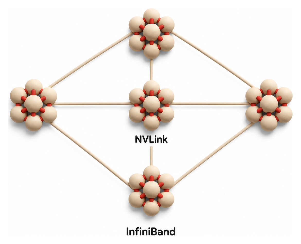
Quantitatively, the gap is large. The current Quantum-X800 InfiniBand platform, used to scale out both GB200/GB300 and Vera Rubin NVL72 racks, provides 800 Gb/s (100 GB/s) of bandwidth per switch port, delivered across 144 ports per switch distributed over 72 octal small form-factor pluggable (OSFP) cages [9] [30]. A two-tier Quantum-X800 fat-tree topology can support over 10,000 800 Gb/s host connections, and the platform's fourth-generation SHARP implementation can boost in-network reduction performance by up to 9x over unaccelerated collectives; the switches also add self-healing technology and telemetry-based congestion control intended to sustain nearly perfect effective bandwidth in multi-tenant, multi-job environments [30]. That is roughly 100 GB/s per port, a small fraction of NVLink 5's 1,800 GB/s or NVLink 6's 3,600 GB/s of aggregate per-GPU bandwidth.
Latency and hierarchy tell a similar story. One infrastructure comparison sets NVLink on Hopper-class H100 SXM hardware at 900 GB/s of intra-node GPU-to-GPU bandwidth, versus 400 Gb/s (50 GB/s) for InfiniBand NDR, 200 Gb/s (25 GB/s) for the older InfiniBand HDR generation, and just 12.5 GB/s for 100 Gigabit Ethernet, describing the difference between 900 GB/s and 1.25 GB/s at the low end of that hierarchy as "the difference between if your cluster performs as advertised or not" [31]. The same comparison sets 400G RDMA over Converged Ethernet (RoCE) at roughly 50 GB/s, matching InfiniBand NDR, which is one reason the article treats 400G RoCE and 400G InfiniBand as functionally interchangeable for new scale-out deployments [31]. It further places GPU-to-CPU transfers over PCIe Gen5 x16 at roughly 64 GB/s and Gen4 x16 at roughly 32 GB/s, each shared across every GPU in the node, and CPU-to-CPU interconnects such as Intel UPI or AMD's own Infinity Fabric at only 48 to 51 GB/s per link, an order of magnitude below even NVLink 4, underscoring why AI racks route GPU-to-GPU traffic through NVLink rather than through the host CPU fabric [31]. NVIDIA states NVLink 6 delivers end-to-end GPU-to-GPU latency three times lower than off-the-shelf Ethernet alternatives, with a ten times higher packet rate, inside the scale-up domain [6].
Both InfiniBand and NVLink use NVIDIA's SHARP (Scalable Hierarchical Aggregation and Reduction Protocol) in-network computing technology to accelerate collective operations, but they implement it at different layers. SHARP was originally introduced on InfiniBand switches to offload collective communication operations, such as all-reduce, reduce, and broadcast, from GPUs and CPUs onto the network switch fabric itself, "reducing the amount of transferred data by half" and minimizing what NVIDIA calls "server jitter" [32]. SHARP has since evolved through several generations on InfiniBand, from small-message scientific-computing reductions in SHARPv1, through large-message AI workload support in SHARPv2 (which demonstrated 17% higher BERT training performance in a June 2021 MLPerf submission), to multi-tenant in-network computing in SHARPv3 and, on Quantum-X800, SHARPv4 with support for FP8 precision and new collective operations such as ReduceScatter and ScatterGather [32]. NVLink Switch chips carry an analogous SHARP engine for in-network reductions and multicast acceleration within the scale-up domain itself [1].
The emergence of an open alternative sharpens this comparison further. UALink (Ultra Accelerator Link), backed by a promoter group including AMD, Broadcom, Cisco, Google, HPE, Intel, Meta, and Microsoft, is an open scale-up standard whose 1.0 specification runs at 200 Gbps (roughly 25 GB/s) per lane, lower than NVLink 5's roughly 100 GB/s per-link rate (Source: spheron.network). AMD's implementation compensates with a denser lane topology: AMD disclosed at CES in January 2026 that its MI455X accelerator in a 72-GPU Helios rack delivers approximately 3.6 TB/s of scale-up bandwidth per accelerator, or roughly 260 TB/s at the rack level, which exceeds NVLink 5's 1.8 TB/s per GPU, though these are AMD-disclosed figures not yet independently validated on shipping silicon (Source: spheron.network).
Data Analysis and Evidence
NVIDIA's own financial disclosures put the scale of the interconnect transition in context. In the first quarter of fiscal 2027 (the quarter ended April 26, 2026), NVIDIA reported record total revenue of $81.6 billion, up 85% year over year, with record Data Center revenue of $75.2 billion, up 92% year over year; within that figure, Data Center compute revenue reached $60.4 billion while Data Center networking revenue, the category that includes NVLink Switch, InfiniBand, and Ethernet products, hit a record $14.8 billion, up 199% year over year and up 35% sequentially [10]. Networking revenue growing more than twice as fast as overall Data Center revenue is a leading indicator that scale-up and scale-out interconnect, not just GPU compute, is becoming a larger share of AI infrastructure spend, consistent with the doubling of NVLink bandwidth and the parallel upgrade cycle in InfiniBand and Ethernet products.
One prior quarter's results illustrate the trajectory. In the first quarter of fiscal 2026 (ended a year earlier), NVIDIA reported total revenue of $44.1 billion, up 69% year over year, with Data Center revenue of $39.1 billion, up 73% year over year; management noted that "our breakthrough Blackwell NVL72 AI supercomputer... is now in full-scale production across system makers and cloud service providers" and that "AI inference token generation has surged tenfold in just one year" [33]. Blackwell contributed nearly 70% of data center compute sales that quarter, as the Hopper-to-Blackwell transition neared completion [33]. Comparing the two years shows Data Center revenue nearly doubling year over year even as the underlying architecture and interconnect generation shifted mid-stream.
Market researchers project continued, steep growth in the surrounding interconnect and AI infrastructure markets. Precedence Research sizes the global data center interconnect market (a broader category spanning DWDM, optical transport, and packet switching hardware and software, not NVLink specifically) at $16.31 billion in 2025, growing to $18.73 billion in 2026 and to approximately $64.96 billion by 2035, a compound annual growth rate (CAGR) of 14.82% from 2026 to 2035, driven in large part by "the adoption of cloud-based solutions, the rise of hyperscale data centers, which require robust, high-bandwidth interconnection" [34]. The same research firm finds that the short-haul connectivity segment, the category that best matches intra-rack fabrics like NVLink, "held a dominant position in the market in 2025, due to the necessity of dense, high-bandwidth short-haul fabrics to manage the exponential surge in east-west traffic required for AI clustering" [34], the same east-west traffic pattern that drives demand for larger NVLink domains, while communication service providers held the largest end-user industry share of that same market in 2025 [34]. Separately, Grand View Research projects the broader AI infrastructure market (hardware, software, and services) growing from $35.42 billion in 2023 to $223.45 billion by 2030, a 30.4% CAGR, with the on-premise deployment segment holding the largest revenue share, at 50.0%, in 2023, the deployment model most closely associated with dedicated NVLink-connected training clusters [35]. These figures should be read as directional signals rather than precise forecasts of NVLink-specific spend, since neither research firm isolates NVLink or NVSwitch revenue from the broader interconnect and AI infrastructure categories they track.
On the hardware side, historical NVLink bandwidth growth has been remarkably consistent. From the first NVLink generation in 2016 (160 GB/s per GPU on the Tesla P100) to NVLink 6 in 2026 (3,600 GB/s per GPU on Rubin), bandwidth increased roughly 22.5 times over ten years, an implied compound annual growth rate of approximately 37% [8]. Scale-up domain size has grown even faster in relative terms over a shorter window: from 8 GPUs in the Hopper-era DGX H100 SuperPOD scalable unit to 72 GPUs in the Blackwell and Rubin NVL72 racks, a nine-fold increase in roughly two years.
NVIDIA describes this rack as functioning like "one massive GPU," with each B200 GPU inside the NVL72 domain able to reach any of the other 71 GPUs at the full 1.8 TB/s NVLink rate
Case Studies and Real-World Examples
CoreWeave: Sequential Adoption of GB200, GB300, and Vera Rubin NVL72
CoreWeave has served as NVIDIA's earliest large-scale commercial adopter across three consecutive NVLink generations. It began offering NVIDIA HGX H100 and H200 systems in 2024, was among the first to demonstrate GB200 NVL72 systems, and then followed with an "industry-first bring-up" of the GB300 NVL72 platform in partnership with Dell Technologies and data center operator Switch, later publishing early projections for Vera Rubin NVL72 as well [15]. Its GB200 NVL72 rollout is paired with CoreWeave's own orchestration stack, including CoreWeave Kubernetes Service and Slurm on Kubernetes, delivered "with performance and reliability" the company says is purpose-built to keep the fabric's advertised bandwidth translating into delivered training throughput [16]. CoreWeave's GB300 NVL72 systems unify 72 Blackwell Ultra GPUs, 36 Grace CPUs, and 18 BlueField-3 DPUs, with NVIDIA Quantum-X800 InfiniBand and ConnectX-8 SuperNICs delivering 800 Gb/s of dedicated network connectivity to each GPU [15]. That deployment sits inside data center operator Switch's AI Factory environment, which the two companies describe as "uniquely engineered to deliver the high power, cooling and operational efficiency required for the most advanced AI workloads" [22]. This sequential adoption pattern, from H100 (NVLink 4) to GB200 (NVLink 5) to GB300 (NVLink 5, Blackwell Ultra) to early Vera Rubin (NVLink 6), makes CoreWeave one of the clearest single-provider timelines for observing the practical rollout cadence of successive NVLink generations.
Microsoft Fairwater: NVLink 5 at Hyperscale Campus Scale
Microsoft's Fairwater datacenters, first built in Mount Pleasant, Wisconsin and later replicated in Atlanta, run on NVIDIA GB200 NVL72 rack-scale systems. Rather than treating each rack as an isolated unit, Microsoft has connected the sites into an "AI superfactory," explaining that "a traditional datacenter is designed to run millions of separate applications for multiple customers," whereas "the reason we call this an AI superfactory is it's running one complex job across millions of pieces of hardware" [19]. This illustrates how NVLink's 72-GPU domain size functions as the fundamental building block that scale-out network design must then multiply across sites, rather than as the final ceiling on cluster size.
xAI Colossus: NVLink 5 in the Largest Single-Coherent Cluster
xAI's Colossus facility in Memphis, Tennessee, reached approximately 2 gigawatts of power capacity and over 555,000 GPUs by January 2026, following a third-building expansion that Jensen Huang reportedly called "superhuman," with construction completed in roughly 19 days versus a typical multi-year timeline [21]. Independent analysis from SemiAnalysis, tracking the facility's build-out, described Colossus 1 as combining "roughly 200,000 H100/H200s and ~30,000 GB200 NVL72" GPUs and, as of that assessment, "the largest fully operational, single-coherent cluster" globally, apart from providers like Google that use distributed multi-datacenter training approaches [20]. Colossus illustrates the largest observed real-world deployment of NVLink 5-based GB200 NVL72 racks operating as part of a single, cohesive training system, though at cluster scale the GB200 NVL72's 72-GPU NVLink domains are themselves stitched together over InfiniBand or Ethernet scale-out fabric rather than a single continuous NVLink fabric.
NVLink Fusion and AWS Trainium4: Extending NVLink Beyond NVIDIA Silicon
Not every case study involves NVIDIA GPUs exclusively. In December 2025, at AWS re:Invent, Amazon Web Services announced a collaboration with NVIDIA to integrate NVLink Fusion, NVIDIA's technology for connecting third-party custom silicon to the NVLink scale-up fabric, with AWS's new Trainium4 AI chips and Graviton CPUs; AWS is designing Trainium4 specifically "to integrate with NVLink 6 and the NVIDIA MGX rack architecture," described as "the first of a multigenerational collaboration between NVIDIA and AWS for NVLink Fusion" [36]. NVLink Fusion provides "a scalable, high-bandwidth networking solution that connects up to 72 custom ASICs with NVIDIA's sixth generation NVLink Switch," meaning hyperscalers building their own accelerators can tap NVLink 6's scale-up fabric without adopting NVIDIA GPUs wholesale [36]. Technical deep-dives on the earlier, fifth-generation implementation describe how custom hardware integrates via the Universal Chiplet Interconnect Express (UCIe) interface, with NVIDIA providing a bridge chiplet for connection to the NVLink fabric, and note that the fifth-generation NVLink underpinning it "supports 72-GPU topologies delivering 1,800 Gb/s bandwidth and 130 Tb/s of aggregate bandwidth," with co-packaged optics versions of both Spectrum-X and the InfiniBand-based Quantum-X fabric planned to extend that photonic integration into NVLink Fusion as well [37]. NVLink Fusion was first unveiled in May 2025 with initial partners MediaTek, Marvell, Alchip Technologies, Astera Labs, Synopsys, and Cadence building custom AI silicon around the NVLink ecosystem, alongside Fujitsu and Qualcomm building custom CPUs to pair with NVIDIA GPUs [38]. This case demonstrates that the NVLink 5-to-6 transition is not confined to NVIDIA's own GPU roadmap; it also sets the terms for how competing accelerator vendors can plug into NVIDIA's scale-up ecosystem.
Implications and Future Directions
The NVLink 5-to-6 transition sits inside a broader multi-year roadmap that NVIDIA has telegraphed well in advance. Beyond Rubin, NVIDIA has already disclosed the Rubin Ultra NVL576 rack, planned for the second half of 2027, which will use a seventh NVLink generation delivering 1.5 PB/s of NVLink bandwidth at the rack level, alongside 4.6 PB/s of HBM4e memory bandwidth and 365 TB of fast memory, in a liquid-cooled "Kyber Rack" design consuming approximately 600 kW [39]. The Rubin Ultra NVL576 is projected to offer 15 exaflops of FP4 inference and 5 exaflops of FP8 training, a claimed 14x improvement over the GB300 NVL72 [39]. Under the same die-versus-package counting convention discussed earlier, Rubin Ultra's rack is expected to house 144 physical packages, each containing four GPU dies, for a total of 576 dies in a single domain, the naming logic behind the NVL576 label [28]. NVIDIA further disclosed that NVLink 7 will maintain the same 400G serdes as NVLink 6 but double the port count to 144 ports per GPU, implying another doubling of per-GPU bandwidth on roughly the same two-year cadence [2]. An eighth generation, NVLink 8, is already anticipated for NVIDIA's subsequent Feynman architecture, planned for 2028 [2] [39].
For infrastructure planners, this cadence has several practical implications. First, the annual-to-biennial pace of NVLink generations means that any large capital commitment to a specific rack generation carries a built-in obsolescence horizon of roughly two years before a materially faster successor ships, though production lead times and depreciation schedules for AI infrastructure typically span three to six years, meaning most deployed fleets will run at least one generation behind the current NVLink release for the majority of their service life. Second, the competitive response from the open UALink consortium is narrowing the gap, at least on paper: AMD's MI455X figures suggest the MI400-generation Helios rack "will still be competitive with the VR200 NVL144's NVLink in terms of scale up bandwidth and also has a scale up world size of 72 logical GPUs," according to SemiAnalysis, though the same analysis cautions that the AMD figures are "AMD-disclosed... not independently validated silicon results" [29] (Source: spheron.network). Part of that competitiveness rests on switch supply: the MI400 Series scale-up network is expected to use Broadcom Ethernet Tomahawk 6 switches because Marvell and Astera Labs' dedicated UALink switches were not expected to be ready until late 2026 [29]. The same SemiAnalysis research notes that AMD's own MI300X would need a one-month rental price of roughly $2.10 to $2.40 per hour to match Nvidia H200 pricing on a performance-per-dollar basis for reasoning inference tasks, a reminder that interconnect quality feeds directly into cloud rental economics rather than remaining an abstract engineering detail [29].
Third, NVIDIA's decision to open NVLink Fusion to third-party custom silicon signals an acknowledgment that not every hyperscaler will standardize on NVIDIA GPUs exclusively, even as they continue relying on NVIDIA's scale-up fabric and its software ecosystem (CUDA, NCCL, NVSHMEM, Dynamo, TensorRT-LLM). This positions NVLink itself, independent of NVIDIA's own GPU sales, as a strategic asset and potential long-term revenue stream as custom ASIC deployment grows across the largest cloud providers. Finally, the resiliency features introduced with NVLink 6, control plane resilience, hot-swappable trays, and partial-rack operation, reflect a broader industry shift toward treating AI factories as continuously operating production infrastructure rather than research clusters, a shift that will likely define feature priorities in NVLink 7 and beyond as much as raw bandwidth does.
Frequently Asked Questions (FAQs)
What is the bandwidth difference between NVLink 5 and NVLink 6? NVLink 5 delivers 1,800 GB/s (1.8 TB/s) of bidirectional bandwidth per GPU across 18 links, while NVLink 6 delivers 3,600 GB/s (3.6 TB/s) per GPU across 36 links, exactly double (see Table 1 above) [13].
What is NVLink 6 bandwidth at the rack level? In the Vera Rubin NVL72 rack, NVLink 6 provides 260 TB/s of aggregate GPU-to-GPU bandwidth across 72 GPUs, plus 130 TFLOPS of FP8 in-network compute for collective operations (see NVLink 6 Capabilities above).
What is NVLink 5 bandwidth at the rack level? In the GB200 and GB300 NVL72 racks, NVLink 5 provides 130 TB/s of aggregate GPU-to-GPU bandwidth across 72 GPUs (see NVLink 5 Capabilities above).
What is the NVLink scale-up domain size, and has it changed between NVLink 5 and NVLink 6? The scale-up domain, the number of GPUs that communicate over the NVLink Switch fabric at full bandwidth without leaving the rack, is 72 GPUs for both the NVLink 5-based GB200/GB300 NVL72 and the NVLink 6-based Vera Rubin NVL72, up from 8 GPUs in the Hopper-era NVLink 4 generation [23]. NVIDIA has signaled further expansion of scale-up domain sizes in systems beyond Vera Rubin, though it has not published a specific figure for a shipping product as of July 2026.
How do NVLink generations compare overall? Per-GPU bandwidth has doubled with nearly every generation: 160 GB/s (NVLink 1, 2016), 300 GB/s (NVLink 2, 2017), 600 GB/s (NVLink 3, 2020), 900 GB/s (NVLink 4, 2022), 1,800 GB/s (NVLink 5, 2024), and 3,600 GB/s (NVLink 6, 2026), as detailed in the Data Analysis section above.
How does NVLink compare to InfiniBand? NVLink is a scale-up fabric operating inside a single rack-scale domain (up to 3.6 TB/s per GPU on NVLink 6), while InfiniBand is a scale-out fabric connecting racks and data center pods together at up to 800 Gb/s (100 GB/s) per switch port on the current Quantum-X800 platform, roughly an order of magnitude lower bandwidth per link but with far greater reach [9].
What GPU uses NVLink 6? NVLink 6 is used by NVIDIA's Rubin-generation GPUs, including the standalone Rubin GPU (also called R200) used in DGX Rubin NVL8 servers and Vera Rubin NVL72 racks, as detailed above.
Is NVLink 6 available yet? As of July 2026, Vera Rubin NVL72 (NVLink 6) has entered full production, with shipments to major cloud partners expected to begin in the second half of 2026; independent, third-party performance benchmarks were not yet publicly available at that point [26] [24].
What comes after NVLink 6? NVIDIA has disclosed NVLink 7, planned for the Rubin Ultra NVL576 rack in the second half of 2027, delivering 1.5 PB/s of NVLink bandwidth at rack scale using the same 400G serdes as NVLink 6 but double the port count, and NVLink 8, anticipated for the Feynman architecture in 2028 [39].
How does NVLink 6 compare to UALink, AMD's open interconnect alternative? NVLink 6 is projected at roughly 2.4 TB/s per GPU in early third-party estimates, though NVIDIA's own figure of 3.6 TB/s is the vendor-disclosed number this report uses throughout; UALink 1.0 is specified at 200 Gbps (about 25 GB/s) per lane, lower per-lane than NVLink, with AMD's MI455X claiming approximately 3.6 TB/s of aggregate scale-up bandwidth per accelerator through a denser lane topology rather than a faster per-lane rate (Source: spheron.network).
Conclusion
NVLink 5 and NVLink 6 represent consecutive steps in a scale-up interconnect roadmap that has doubled GPU-to-GPU bandwidth roughly every two years since 2016. NVLink 5, announced with Blackwell in 2024, delivers 1.8 TB/s of per-GPU bandwidth and 130 TB/s of aggregate rack bandwidth across a 72-GPU domain. GB200 NVL72 systems became available to customers at scale in 2025, and NVIDIA expected Blackwell Ultra products, including GB300 NVL72, from partners beginning in the second half of 2025. NVLink 6, arriving with the Rubin platform and its flagship Vera Rubin NVL72 rack, doubles per-GPU bandwidth to 3.6 TB/s and aggregate rack bandwidth to 260 TB/s within the same 72-GPU domain size, while adding substantial operational resiliency features and roughly doubling in-network compute for accelerating collective communication.
For organizations planning cluster purchases or cloud capacity commitments today, the practical choice is less "NVLink 5 versus NVLink 6" in the abstract and more a question of availability, workload fit, and risk tolerance. NVLink 5 systems have production operating experience and independent MLPerf submissions; GB200 NVL72 systems became available to customers at scale in 2025. NVLink 6 systems offer materially higher bandwidth and better resiliency, directly relevant to the largest mixture-of-experts and long-context reasoning workloads, but as of July 2026 remain in the early stages of production shipment, with performance claims still resting primarily on NVIDIA's own simulations rather than independently verified benchmarks. Both generations exist strictly as scale-up fabrics, complementary to rather than competitive with InfiniBand and Ethernet scale-out networking, and both face a narrowing bandwidth gap from the open UALink standard promoted by AMD and its consortium partners. Buyers evaluating either generation should weigh workload communication intensity, deployment timeline, and the maturity of independent performance validation alongside the headline bandwidth figures this report has detailed.
External Sources (39)
About
GPUSmith
Plan and build private AI compute with GPU Smith. We connect workload requirements with GPU hardware, networking, deployment and operating decisions so your infrastructure fits the work it must perform.
GPU Smith provides independent engineering and research for private AI infrastructure. We help technical buyers and operators reason about GPU workload sizing, hardware selection, procurement, deployment and inference operations, from the compute system to the networking, power and cooling requirements around it.
Start with the workload
Useful infrastructure decisions begin with the models, data, throughput, latency and operating constraints a team actually has. GPU Smith helps connect those requirements with system design and deployment choices. The goal is a privately controlled AI environment whose capacity and operational demands are understood before a purchasing decision.
Hardware and supplier research
Our public reference library covers GPUs, complete systems and networking components. The server-vendor directory and manufacturing research help teams investigate suppliers, compare options and follow sources behind technical claims. We distinguish manufacturer specifications from measured benchmarks and advertised capabilities from tested configurations. Reference pages are research resources, not a live inventory listing or a binding equipment quote.
Deployment and operations
GPU Smith's engineering scope includes infrastructure integration, networking, power, cooling and the practical operation of inference workloads. Our published articles explain the tradeoffs behind deployment, procurement and ongoing operations so teams can ask better questions and document decisions.
Work with GPU Smith
Explore the hardware library, GPU references, networking references and vendor research. Contact GPU Smith with your workloads and deployment constraints to discuss a project and confirm current scope, pricing and availability.
Inclusion of a manufacturer or product in our research does not imply a partnership, certification or endorsement.
Disclaimer
This document is provided for informational purposes only. No representations or warranties are made regarding the accuracy, completeness, or reliability of its contents. Any use of this information is at your own risk. GPUSmith shall not be liable for any damages arising from the use of this document. This content was generated with assistance from artificial intelligence tools, which may contain errors or inaccuracies. Readers should verify critical information independently. All product names, trademarks, and registered trademarks mentioned are property of their respective owners and are used for identification purposes only. Use of these names does not imply endorsement. This document does not constitute professional or legal advice. For specific guidance related to your needs, please consult qualified professionals.