GPUSmith Article
NVIDIA NVLink vs AMD Infinity Fabric: 2026 Interconnect Guide
Summary
- 01NVIDIA's fifth-generation NVLink delivers 1.8 TB/s per Blackwell GPU and scales via NVSwitch to 130 TB/s aggregate bandwidth across the 72-GPU GB200 NVL72 rack.
- 02AMD's fourth-generation Infinity Fabric links MI300X's eight GPUs at 128 GB/s per link for 896 GB/s of aggregate bandwidth, with no shipping rack-scale switch fabric yet.
- 03These bandwidth figures have different scopes and should not be presented as a like-for-like 2x per-GPU comparison between NVIDIA and AMD.
- 04UALink's 1.0 specification, ratified April 2025, supports pods of up to 1,024 accelerators at 200 Gbps per lane, offering the first serious open alternative to proprietary scale-up fabrics.
- 05AMD's Data Center segment grew 57% year over year to $5.8 billion in Q1 2026, while AMD agreed to sell up to $60 billion of AI chips to Meta over five years.
- 06650 Group forecasts scale-up switching revenue will exceed $30 billion by 2030, with an estimated $25 billion of that going to NVLink.
Inside this article
NVIDIA NVLink vs AMD Infinity Fabric: 2026 Interconnect Guide
Executive Summary
NVIDIA NVLink and AMD Infinity Fabric are the two dominant proprietary interconnect technologies that let multiple GPUs act as a single, larger accelerator, and the choice between them (or the emerging open standards challenging both) increasingly determines whether an AI cluster can train trillion-parameter models efficiently. As of July 2026, NVIDIA's fifth-generation NVLink delivers 1.8 TB/s of bidirectional bandwidth per Blackwell GPU, and when paired with fifth-generation NVLink Switch it scales to 130 TB/s of aggregate bandwidth across the 72-GPU GB200 NVL72 rack [1]. AMD's fourth-generation Infinity Fabric, by contrast, links the eight GPUs inside an Instinct MI300X server at 128 GB/s per peer-to-peer link, for 896 GB/s of aggregate bandwidth in a fully connected 8-GPU node [2] [3]. These figures have different scopes: NVIDIA lists 1.8 TB/s per Blackwell GPU, while AMD lists 128 GB/s per Infinity Fabric link and 896 GB/s of aggregate bidirectional peer-to-peer I/O for an MI300X OAM. They should not be presented as a like-for-like 2x per-GPU comparison. The architectural difference is that NVLink 5 uses an added switch layer (NVSwitch) to create a non-blocking, rack-scale fabric, while AMD's shipping Instinct products directly connect GPUs within an 8-GPU node and use external networking to scale between nodes.
This report also answers the cluster of related questions buyers and engineers are asking in 2026: how NVSwitch differs from NVLink itself (it is the switching silicon, not the link, providing an 18-port non-blocking crossbar with 50 GB/s of bidirectional bandwidth per port, or 900 GB/s of aggregate switch bandwidth) [4]; how the new Ultra Accelerator Link (UALink) open standard, ratified at 200 Gbps per lane in its 1.0 specification in April 2025, aims to give non-NVIDIA accelerators a shared scale-up fabric for pods of up to 1,024 accelerators [5]; and how Ultra Ethernet (UEC Specification 1.0, released June 11, 2025) and traditional InfiniBand compare for scale-out networking between nodes and racks [6].
The competitive and financial stakes are large. NVIDIA reported record Data Center revenue of $62.3 billion for the fourth quarter of fiscal 2026 alone, and $193.7 billion for the full fiscal year, up 68% year over year, a scale of business built substantially on the NVLink-tied GB200 and GB300 NVL72 platforms [7]. AMD's Data Center segment, powered by Instinct MI300X, MI325X, MI350X, and MI355X GPUs connected by Infinity Fabric, grew 57% year over year to $5.8 billion in the first quarter of 2026, and AMD has since agreed to sell up to $60 billion of AI chips to Meta over five years in a deal that also gives Meta the option to buy up to 10% of AMD [8] [9].
The report's core conclusion is that NVLink has a rack-scale topology advantage in shipping products: NVSwitch enables a non-blocking 72-GPU domain, while AMD's currently documented Instinct systems directly connect GPUs within an 8-GPU node. AMD's Helios roadmap targets larger domains. Meanwhile, the scale-out layer, the network connecting racks and pods together, is undergoing its own transition as Ultra Ethernet and Broadcom's Tomahawk Ultra switch (250 nanosecond latency at 51.2 Tbps) challenge InfiniBand's historical dominance, and UALink offers the first serious open alternative to proprietary scale-up fabrics for accelerators beyond NVIDIA's own lineup [10]. Buyers choosing an AI cluster architecture in 2026 face a genuinely bifurcated market: NVLink for maximum single-vendor performance density, Infinity Fabric plus open standards for multi-vendor flexibility and cost control.
Introduction and Background
Modern large language model training and inference no longer run on a single graphics processing unit (GPU). A model with hundreds of billions or trillions of parameters must be split across dozens, hundreds, or thousands of GPUs, and the speed at which those GPUs exchange intermediate results, gradients, and activations often matters more than the raw compute of any individual chip. This is the role of a GPU interconnect: a dedicated, high-bandwidth communication fabric that lets multiple accelerators behave, from the software's perspective, as one much larger device. NVIDIA NVLink and AMD Infinity Fabric are the two most consequential proprietary answers to this problem, and the question of which is faster, more scalable, or more cost-effective sits at the center of nearly every large AI infrastructure procurement decision made in 2026.
The stakes have risen sharply because model architectures have shifted toward mixture-of-experts (MoE) designs, which require frequent all-to-all communication between GPUs holding different "experts," and toward test-time reasoning models that demand low-latency inference across many chips simultaneously. NVIDIA's own technical documentation for the GB200 NVL72 frames the challenge directly, noting that for GPUs "to work in parallel efficiently, so they must communicate with high bandwidth and low latency and keep constantly busy," a requirement that motivated the entire rack-scale NVLink Switch System design [11]. In this environment, an interconnect that is even modestly faster or lower-latency can translate directly into shorter training runs, cheaper inference, and higher utilization of expensive accelerator silicon. Because accelerator hardware itself is extremely expensive, any interconnect bottleneck that leaves GPUs idle while waiting for data effectively wastes capital that has already been spent, which is why infrastructure teams increasingly treat interconnect bandwidth as a first-order procurement criterion rather than a footnote on the GPU spec sheet.
NVLink originated with NVIDIA's Pascal architecture in 2016, offering 160 GB/s of bidirectional bandwidth per GPU in its first generation, connecting GPUs directly to each other and to IBM POWER8+ CPUs [12]. AMD's Infinity Fabric traces its lineage to the first Zen CPU architecture in 2017, where it served initially as an on-die and inter-die interconnect for AMD's chiplet-based Ryzen and EPYC processors, before AMD extended it to GPU-to-GPU and CPU-to-GPU communication in the Instinct accelerator line beginning with the MI200 series. Both technologies exist because the industry-standard alternative, PCI Express (PCIe), was never designed for the volume or latency profile that multi-GPU AI training demands; even PCIe 5.0 tops out at roughly 126 GB/s of aggregate bidirectional bandwidth per x16 slot, an order of magnitude below what a modern 8-GPU NVLink or Infinity Fabric domain can move [12]. This report examines both technologies in depth, covers the switch silicon that extends them beyond a single server (NVSwitch on the NVIDIA side), surveys the emerging open standards, UALink and Ultra Ethernet, that are trying to break vendor lock-in at the scale-up and scale-out layers respectively, and compares the older InfiniBand networking standard against these newer approaches. It draws on vendor documentation, national laboratory system guides, standards-body specifications, financial filings, wire-service reporting, and independent technical analyses current as of July 2026; readers should evaluate each linked source in the context of the claim it supports. Readers should come away with a clear, quantified answer not only to "NVLink vs Infinity Fabric" but to the broader question of how the AI interconnect stack is being reorganized around open standards in 2026.
NVIDIA NVLink
Capabilities
NVLink is NVIDIA's proprietary, high-speed, point-to-point interconnect for GPU-to-GPU and CPU-to-GPU communication, first introduced with the Pascal architecture. Each generation has roughly doubled per-link and per-GPU bandwidth. The first generation delivered 20 GB/s per sub-link with four links per GPU for 160 GB/s total, using Pascal GPUs paired with IBM's POWER8+ CPUs [12]. The second generation, introduced with Volta, raised the per-sub-link rate to 25 GB/s and added a sixth link, reaching 300 GB/s per GPU [12]. NVLink 3.0, announced May 14, 2020 for the Ampere architecture, doubled the per-pair data rate to 50 Gbit/s while halving pairs per sub-link, and added more links (12) for a total of 600 GB/s per A100 GPU [12]. NVLink 4.0, paired with the Hopper architecture announced in March 2022, added six more links (18 total) at the same 50 GB/s per-link rate, reaching 900 GB/s per H100 GPU [12].
The current, fifth generation, shipping with the Blackwell architecture, has 18 links and delivers 1,800 GB/s (1.8 TB/s) of total bidirectional bandwidth per GPU. That total corresponds to 100 GB/s bidirectional per link—50 GB/s in each direction—which NVIDIA states is 14x the bandwidth of PCIe Gen5 [12] [1]. An independent technical breakdown of the architecture confirms that within a single NVL72 rack, "each GPU has 18 NVLink ports and each rack has 18 NVSwitches, each GPU can connect to each NVSwitch in the rack to form a single-layer, non-blocking fabric" [13], and that NVLink Switch trays in this generation carry "72x400G ports" of switching capacity per tray [13]. NVIDIA has already previewed a sixth generation for its upcoming Rubin platform, promising 3.6 TB/s of bandwidth per GPU, another 2x jump, using 36 links per GPU [14].
- NVSwitch: the companion switch silicon that extends point-to-point NVLink into a fully non-blocking, all-to-all fabric. The original NVSwitch enabled 16 GPUs at 300 GB/s each in a single node, described by NVIDIA as "the World's Highest-Bandwidth On-Node Switch" [4]. Each NVSwitch chip is an 18x18-port fully connected crossbar where any port can talk to any other port at full NVLink speed [4]. The Hopper-generation NVLink 4 Switch scaled to 7.2 TB/s total aggregate bandwidth across an 8-GPU domain [14].
- NVLink Switch System: the rack-scale extension of NVSwitch, first deployed at scale in the GB200 NVL72, connecting 72 Blackwell GPUs into one NVLink domain delivering 130 TB/s of aggregate low-latency GPU communication bandwidth, the largest single-rack NVLink domain NVIDIA has offered to date. NVIDIA's own technical blog notes that fifth-generation NVLink can extend further still, "connecting up to 576 GPUs in a single NVLink domain with over 1 PB/s total bandwidth" when spanning multiple racks [11], a figure consistent with the 576-GPU-per-pod ceiling referenced later in this report's discussion of UALink. The follow-on GB300 NVL72, built around Blackwell Ultra GPUs, carries the same 130 TB/s NVLink bandwidth figure while adding 1.5x more dense FP4 Tensor Core throughput [15].
- SHARP in-network computing: each NVLink Switch chip also incorporates engines for NVIDIA's Scalable Hierarchical Aggregation and Reduction Protocol (SHARP), which performs in-network reductions and multicast acceleration, so that collective operations such as AllReduce are partly computed inside the switch fabric itself rather than solely on the GPUs, reducing the data volume that must traverse the network for large collective training operations [14].
- NVLink-C2C: a separate chip-to-chip interconnect variant used to fuse a Grace CPU and a Hopper or Blackwell GPU into a single coherent memory space, delivering 900 GB/s of total bandwidth between the Grace CPU and Hopper GPU in the GH200 Grace Hopper Superchip [16] and 1 TB/s of memory bandwidth for the Grace CPU Superchip's dual-die configuration [17]. Each GB200 compute tray built on this design "delivers 80 petaflops of AI performance and 1.7 TB of fast memory," according to NVIDIA's developer documentation [11].
- NVLink Fusion: announced May 18, 2025, a program that opens NVLink and NVLink-C2C intellectual property to third-party silicon designers, letting hyperscalers integrate custom ASICs or CPUs with NVIDIA GPUs. Early adopters include MediaTek, Marvell, Alchip Technologies, Astera Labs, Synopsys, and Cadence for custom AI silicon, and Fujitsu and Qualcomm Technologies for custom CPUs [18].
First generation delivered 160 GB/s total using Pascal GPUs paired with IBM POWER8+ CPUs.
Second generation raised the per-sub-link rate to 25 GB/s and added a sixth link, reaching 300 GB/s per GPU.
Announced May 14, 2020, doubled the per-pair data rate and reached 600 GB/s per A100 GPU.
Announced March 2022, added six more links for a total of 18, reaching 900 GB/s per H100 GPU.
Current fifth generation, shipping with Blackwell, has 18 links and delivers 1,800 GB/s of total bidirectional bandwidth per GPU.
NVIDIA has previewed a sixth generation promising 3.6 TB/s of bandwidth per GPU using 36 links per GPU.
the king of inference today, delivering an order-of-magnitude lower cost per token
Adoption
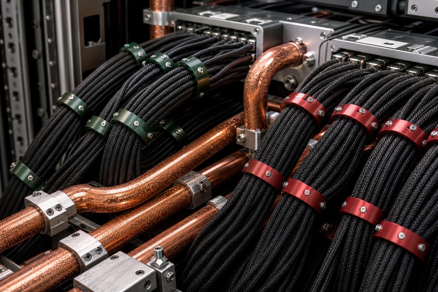
NVLink's clearest large-scale showcase is the GB200 NVL72, which packages 36 Grace CPUs and 72 Blackwell GPUs into a single liquid-cooled rack, described by NVIDIA as "an exascale computer in a single rack" [1]. CoreWeave became the first cloud provider to announce general availability of GB200 NVL72 instances on February 4, 2025, and the first hyperscaler to deploy the follow-on GB300 NVL72 platform on July 3, 2025 [19]. CoreWeave's GB200 deployment combines rack-level NVLink connectivity with NVIDIA Quantum-2 InfiniBand networking delivering 400 Gb/s bandwidth per GPU across clusters scaling up to 110,000 GPUs [19], a concrete illustration of how NVLink (scale-up, inside the rack) and InfiniBand (scale-out, between racks) function as complementary rather than competing layers. NVIDIA's own materials add that the NVL72's copper cable cartridge and liquid-cooling design together deliver "25x lower cost and energy consumption" relative to prior air-cooled architectures [11]. NVIDIA's Q4 fiscal 2026 results describe Grace Blackwell with NVLink as "the king of inference today, delivering an order-of-magnitude lower cost per token," in the words of founder and CEO Jensen Huang [7]. The GB300 NVL72's accompanying Grace CPU is described by NVIDIA as delivering "outstanding performance and memory bandwidth with 2x the energy efficiency of today's leading server processors" [15], while the platform's Mission Control software "powers every aspect of NVIDIA GB300 NVL72 AI factory operations, from orchestrating workloads across the 72-GPU NVLink domain" to facility-level integration [15].
NVIDIA's overall data center dominance underpins NVLink's reach: independent market trackers place NVIDIA's share of AI accelerator or discrete GPU shipments at roughly 80 to 92 percent as of 2025, though figures vary by methodology and whether they measure unit shipments or revenue [20]. NVIDIA's own Data Center segment revenue of $193.7 billion for fiscal 2026 (up 68% year over year) reflects how much of the AI compute buildout runs through NVLink-connected systems [7].
Strengths and Limitations
NVLink's principal strength is bandwidth density combined with genuine all-to-all topology at rack scale: the 130 TB/s NVL72 domain lets 72 GPUs behave, for many purposes, as one very large accelerator, which is particularly valuable for mixture-of-experts models whose expert-routing communication pattern is inherently all-to-all. Its principal limitation is that it remains a proprietary NVIDIA technology; even with the NVLink Fusion licensing program opening the door to third-party CPUs and ASICs, the core GPU compute remains NVIDIA silicon, and customers seeking a fully open, multi-vendor scale-up fabric must look to UALink or Ethernet-based alternatives instead.
AMD Infinity Fabric
Capabilities
Infinity Fabric is AMD's proprietary interconnect, used both within and between chips, spanning CPU core-to-core communication, CPU-to-GPU links, and GPU-to-GPU links. On the Instinct accelerator side, the technology has gone through several packaging and bandwidth iterations. The MI200 series (specifically MI250X), which powers the Frontier supercomputer, connects the two Graphics Compute Dies (GCDs) inside a single MI250X package via Infinity Fabric GPU-GPU at 200 GB/s of bandwidth in each direction simultaneously, while GCDs on different MI250X packages within a node connect at 50 to 100 GB/s depending on the number of Infinity Fabric links between them [21].
The MI300X, built on CDNA 3 architecture, uses fourth-generation Infinity Fabric to fully interconnect eight GPUs, each Infinity Fabric link delivering 128 GB/s of peak bandwidth, for a total of 896 GB/s across the fully connected 8-GPU topology [3] [2]. Each MI300X GPU also carries eight Infinity Fabric links and a separate PCIe 5.0 x16 host connection [3]. Within the MI300X package itself, an Infinity Fabric Advanced Package link connects the constituent chiplets (four I/O dies and eight Accelerator Complex Dies) with 4.8 TB/s of bisection bandwidth [2], separate from and much faster than the chip-to-chip fabric linking discrete GPUs.
The newer MI350 series (MI350X and MI355X, fourth-generation CDNA architecture) continues to use "AMD Infinity Fabric Link enabling high-bandwidth GPU-to-GPU communication while maintaining Universal Base Board (UBB 2.0) compatibility" [22], while the MI355X carries 288 GB of HBM3E memory at 8 TB/s peak memory bandwidth [23]. AMD's roadmap points toward the MI450 generation and the Helios rack-scale architecture, developed jointly with Meta through the Open Compute Project, as the vehicle for a larger, rack-scale Infinity Fabric domain intended to compete more directly with NVL72-class systems [24]. Reuters reporting on the AMD-Meta agreement adds a technical detail relevant to that roadmap: "Meta helped contribute to the MI450 design that is optimized for a computing process known as inference," positioning the chip to compete directly with NVIDIA's next-generation Vera Rubin processor [9].
- Chiplet coherence: Infinity Fabric also underlies AMD's MI300A accelerated processing unit (APU), which integrates 24 Zen 4 x86 CPU cores with 228 CDNA 3 GPU compute units and 128 GB of unified HBM3 memory in a single coherent package, the design at the heart of the El Capitan supercomputer [25].
- CPU-GPU host bandwidth: on Frontier, the CPU-to-GCD Infinity Fabric CPU-GPU link provides 36+36 GB/s of simultaneous host-to-device and device-to-host bandwidth [21]. Wikipedia's technical summary of Frontier corroborates this coherence model, noting that the system "has coherent interconnects between CPUs and GPUs, allowing GPU memory to be accessed coherently by code running on the Epyc CPUs" [26].
Adoption
Infinity Fabric's most prominent showcase is scientific computing rather than commercial cloud rental. The Frontier supercomputer at Oak Ridge National Laboratory uses 9,408 AMD EPYC "Trento" CPUs and 37,632 Instinct MI250X accelerator modules connected via Infinity Fabric, and became the world's first system to exceed one exaFLOP of sustained performance [26]. El Capitan, AMD's follow-on system at Lawrence Livermore National Laboratory, subsequently overtook Frontier and held the title of world's fastest supercomputer on the TOP500 list from November 2024 until June 2026, when it was displaced by a newer system; as of the June 2026 list, El Capitan ranks second worldwide, and Frontier has fallen further down the rankings, though both remain among the most powerful Infinity Fabric-connected systems in production [27]. El Capitan, built by Hewlett Packard Enterprise, uses 43,808 AMD Instinct MI300A GPUs paired with an equal number of fourth-generation EPYC "Genoa" CPUs for the U.S. National Nuclear Security Administration's stockpile stewardship mission [27].
On the commercial side, AMD's Data Center segment revenue reached $5.8 billion in the first quarter of 2026, up 57% year over year, which AMD attributed to "strong demand for AMD EPYC processors and the continued ramp of AMD Instinct GPU shipments" [8]. In the largest single commercial commitment tied to Infinity Fabric-connected hardware to date, Reuters reported that AMD "agreed to sell up to $60 billion worth of artificial intelligence chips to Meta Platforms over five years in a deal that allows the Facebook owner to purchase as much as 10% of the chip firm," with the first gigawatt of shipments, based on a custom MI450-architecture GPU and AMD's Helios rack-scale design, scheduled to begin in the second half of 2026 [9]. As part of the agreement, AMD is issuing Meta a warrant for 160 million shares with an exercise price of one cent, vesting as AMD's stock price hits rising performance targets and as Meta reaches technical and commercial milestones. AMD's Infinity Fabric-based footprint also extends into the CPU side of the same hyperscalers: in the same quarter, AMD reported that AWS, Google Cloud, Microsoft Azure, and Tencent all announced new or expanded fifth-generation EPYC-powered cloud instances, including instances "across general-purpose, memory- and compute-optimized workloads," underscoring how the chiplet-based Infinity Fabric architecture underpins both AMD's CPU and GPU product lines across major public clouds rather than only appearing in dedicated supercomputers [8]. IBM has also announced plans to deploy MI300X accelerators as a service on IBM Cloud, expected to become available in the first half of 2025, to support generative AI and high-performance computing workloads for enterprise clients [28].
Meta is locking in supply, diversifying away from a single vendor, and doing whatever it takes to make sure its AI ambitions aren't bottlenecked by chips
Strengths and Limitations
Infinity Fabric's principal strengths are its coherent CPU-GPU memory model, well demonstrated in the MI300A APU design that powers El Capitan, and its cost-competitive positioning: cloud rental prices for MI300X instances have ranged from roughly $0.95 to $7.86 per GPU-hour in 2026, generally undercutting comparable NVIDIA H100 pricing of $1.38 to $8.00-plus per GPU-hour at the low end of the market (Source: spheron.network) [29]. Its principal limitation, as of shipping products in mid-2026, is scale: Infinity Fabric's largest directly connected GPU domain remains an 8-GPU node, reaching up to 1,075.2 GB/s aggregate peer-to-peer bandwidth per MI350-series GPU OAM module. That is far smaller in domain size than NVLink Switch's 72-GPU, 130 TB/s domain, so AMD clusters scaling beyond a single node depend more heavily on external networking (InfiniBand, RoCE, or forthcoming Ultra Ethernet fabrics) to approximate the all-to-all behavior NVLink Switch provides natively within a rack [30].
UALink, Ultra Ethernet, and the Open Standards Challenge
Capabilities
Two industry consortia are attempting to give the market open, multi-vendor alternatives to NVIDIA's proprietary NVLink stack, one addressing scale-up (within-rack, accelerator-to-accelerator) communication and the other addressing scale-out (between-rack, node-to-node) networking.
UALink (Ultra Accelerator Link), founded in May 2024, ratified its 1.0 specification on April 8, 2025. The 1.0 specification "defines a low-latency, high-bandwidth interconnect for communication between accelerators and switches in AI computing pods" and "enables 200G per lane scale-up connection for up to 1,024 accelerators within an AI computing pod." The Consortium now also lists the UALink Common 2.0 Specification as available; it introduces in-network compute for UALink systems. [5]. Consortium membership exceeds 85 companies, including AMD, Intel, Meta, Amazon Web Services, Google, Microsoft, Cisco, Apple, and Hewlett Packard Enterprise [5]. UALink Consortium president Peter Onufryk stated: "With the release of the UALink 200G 1.0 Specification, the UALink Consortium's member companies are actively building an open ecosystem for scale-up accelerator connectivity" [31]. UALink positions itself explicitly "as an alternative to Nvidia's NVLink offering, which at present supports up to 576 GPUs per pod" [31], and its design draws directly on AMD's own interconnect experience, with reporting noting "it is based on AMD's Infinity Fabric" technology [32].
Ultra Ethernet Consortium (UEC), hosted by the Linux Foundation and started by Intel, AMD, Meta, HPE, and others, released its Specification 1.0 on June 11, 2025, described as "a comprehensive, Ethernet-based communication stack engineered to meet the demanding needs of modern Artificial Intelligence (AI) and High-Performance Computing (HPC) workloads" [6]. The specification, which runs over 560 pages, covers NICs, switches, optics, and cables, adds native RDMA (Remote Direct Memory Access) support at the data-link layer, and introduces a new transport protocol called Ultra Ethernet Transport (UET) for intelligent flow control [33]. UEC Steering Committee Chair Dr. J Metz called the release "a major milestone in our mission to redefine Ethernet for the age of AI and high-performance computing" [6].
At the silicon level, Broadcom's Tomahawk Ultra switch, which began shipping July 15, 2025, is built to support both the UALink-adjacent scale-up Ethernet approach and Ultra Ethernet Consortium compliance. It achieves 250 nanosecond switch latency at full 51.2 Tbps throughput, supports up to 77 billion packets per second at minimum 64-byte packet sizes, and, when combined with Broadcom's Scale-Up Ethernet (SUE) specification, enables sub-400 nanosecond XPU-to-XPU communication latency including switch transit time [10]. AMD's Forrest Norrod, Executive Vice President and General Manager of the Data Center Solutions Group, endorsed the approach: "By combining Broadcom's new Tomahawk Ultra switch with AMD Instinct GPUs and EPYC processors, we're enabling high-performance, standards-based Ethernet solutions for AI infrastructure" [10].
Adoption
Market research firm 650 Group forecasts that scale-up switching revenue (the market covering NVLink, UALink, and Ethernet-based scale-up fabrics together) will exceed $30 billion by 2030, broken down into an estimated $25 billion-plus for NVLink, $8 billion-plus for Ethernet-based scale-up, and $3 billion-plus for PCIe/UALink [34], reflecting a market where "almost the entire market is served by NVIDIA's NVLink" today but non-NVIDIA accelerators increasingly need "robust networking fabrics as they look to expand beyond a single server" [34]. The same research forecasts AI scale-out Ethernet revenue exceeding InfiniBand's over the same period, a trend discussed further in Table 2 below. In October 2025, hyperscalers and vendors including AMD and Meta announced Ethernet for Scale Up Networking (ESUN) at the OCP Summit to standardize the lower layers of Ethernet-based scale-up fabrics, an initiative reflecting the same Helios rack-scale collaboration described in the Infinity Fabric adoption discussion above.
Strengths and Limitations
The open standards' core strength is vendor independence: a data center operator using UALink or Ultra Ethernet in principle is not locked into any single accelerator vendor's roadmap for scale-up or scale-out bandwidth, and can mix silicon from multiple suppliers. Their core limitation, as of July 2026, is ecosystem maturity: the Consortium lists UALink 200G 1.0 and Common 2.0 specifications as available, while its FAQ says products using an open standard typically enter the market one to two years after the initial specification release. Both standards must still prove they can match the bandwidth density, software stack maturity (NVIDIA's NCCL collective communication library, Magnum IO, and SHARP in-network computing), and operational track record that NVLink and InfiniBand have accumulated over nearly a decade of production deployment.
Feature Comparison
Table 1 below summarizes the headline bandwidth, scale, and topology characteristics of the major GPU interconnect technologies discussed in this report, drawing on the vendor and standards-body sources cited throughout.
| Technology | Current Generation | Per-GPU / Per-Link Bandwidth | Maximum Domain Size (shipping or specification) | Topology | Governance |
|---|---|---|---|---|---|
| NVIDIA NVLink | NVLink 5 (Blackwell) | 1.8 TB/s per GPU [14] | 72 GPUs at 130 TB/s aggregate (NVL72) [1] | All-to-all via NVSwitch crossbar | Proprietary (NVIDIA); licensable via NVLink Fusion |
| AMD Infinity Fabric | 4th Gen (MI300/MI350 series) | 128 GB/s per link, 896 GB/s aggregate (MI300X, 8 GPU) [3] | 8 GPUs per node (shipping); rack-scale planned via Helios/MI450 | Fully connected node topology | Proprietary (AMD) |
| UALink 1.0 | 200G 1.0 Specification | 200 Gbps per lane [5] | Up to 1,024 accelerators per pod [5] | Switched accelerator fabric | Open standard (UALink Consortium, 85+ members) |
| Ultra Ethernet (UEC 1.0) | Specification 1.0 | Varies by NIC/optics (800G, 1.6T pluggables in roadmap) | Designed to scale to "millions of endpoints" [6] | Scale-out Clos/fat-tree fabric | Open standard (Linux Foundation-hosted UEC) |
| NVIDIA Quantum-X800 InfiniBand | Quantum-X800 | 800 Gb/s per port, 144 ports [35] | Two-level fat-tree, tens of thousands of nodes | Scale-out fat-tree fabric | Industry standard (InfiniBand Trade Association); NVIDIA is a major supplier |
| Broadcom Tomahawk Ultra (Ethernet) | Tomahawk Ultra | 51.2 Tbps switch throughput, 250 ns latency [10] | Rack-scale to data-center scale | UEC-compliant scale-up and scale-out | Merchant silicon (Broadcom); open standards-compliant |
The table makes clear that NVLink's advantage is not merely raw link speed but the combination of speed and topology: NVSwitch provides a non-blocking all-to-all 72-GPU NVLink domain. Each GPU has up to 1.8 TB/s aggregate bidirectional NVLink bandwidth into the rack's 130 TB/s aggregate fabric; this does not mean that 1.8 TB/s is independently available to each of 71 peers at the same time [36]. Infinity Fabric's current MI350-series figure of up to 1,075.2 GB/s aggregate peer-to-peer bandwidth per GPU OAM module, while substantial at the 8-GPU scale, does not yet have a shipping equivalent at rack scale. That is the gap AMD's Helios architecture and the open UALink and Ultra Ethernet standards are trying to close from different directions: AMD through its next-generation hardware and the industry consortia through vendor-neutral specifications that accelerator makers could adopt [30].
Performance and Benchmarks
Direct, apples-to-apples third-party benchmarks comparing NVLink-connected and Infinity Fabric-connected clusters on identical workloads are scarce in the public record as of July 2026, a gap this report notes honestly rather than papering over with vendor claims presented as independent results. Available data instead falls into two categories: vendor-reported comparative claims, and independent competitive benchmark suites such as MLPerf.

On the vendor-claims side, NVIDIA states that GB200 NVL72 delivers 30x faster real-time large language model inference and 4x faster training for large language models at scale compared with the prior Hopper (H100)-based generation, attributing the gains explicitly to the combination of a second-generation Transformer Engine and fifth-generation NVLink, with the underlying test comparing a 4,096-GPU H100 InfiniBand cluster against a 456-GPU GB200 NVL72 cluster running a 1.8 trillion-parameter mixture-of-experts model [1]. CoreWeave's GB200 NVL72 marketing repeats similar comparative figures, "up to 30X faster" inference relative to previous generations, sourced to the identical NVIDIA benchmark methodology rather than an independent measurement [19]. These figures should be read as vendor-reported, workload-specific claims rather than a generalized, interconnect-isolated benchmark. NVIDIA extends the same comparative logic to its GB300 NVL72 platform, which it says delivers "up to a 50x overall increase in AI factory output performance compared to NVIDIA Hopper-based platforms" when paired with Quantum-X800 InfiniBand or Spectrum-X Ethernet networking [15]; CoreWeave's own GB300 rollout separately claims "a 10x boost in user responsiveness" and "a 5x improvement in throughput per watt" versus Hopper for the same platform [37]. As with the 30x and 4x figures above, these remain vendor-reported comparative claims tied to specific workloads rather than independently reproduced benchmarks, a distinction this report maintains throughout because vendor marketing materials and independently verified measurements are not interchangeable evidence.
On the independent side, AMD reports that its MI355X accelerator "delivered strong competitive performance across the full suite, with leadership results in multiple categories" in the latest MLPerf inference benchmark round, an industry-standard, third-party-audited benchmark suite maintained by MLCommons [8]. Because MLPerf submissions report end-to-end system performance rather than isolating interconnect contribution, they cannot cleanly separate the effect of Infinity Fabric bandwidth from GPU compute, memory bandwidth, or software stack maturity (AMD's ROCm versus NVIDIA's CUDA and NCCL).
At the network layer, Meta's own engineering team, publishing in the peer-reviewed proceedings of ACM SIGCOMM 2024, reported that its RDMA over Converged Ethernet (RoCEv2) network achieved "performance improvement of up to 40% for the AllReduce collective" after implementing Enhanced ECMP (E-ECMP) with queue-pair scaling, and that a path-pinning scheme without such optimization had previously caused training performance to degrade "up to more than 30%" under uneven job placement [38]. This is one of the clearest independently documented data points showing that network engineering choices, not just raw interconnect bandwidth specifications, materially affect realized AI training performance, a nuance vendor bandwidth figures alone do not capture. Meta also noted a specific tradeoff versus InfiniBand: "Setting the channel buffer size requires a more careful balance between congestion spreading and bandwidth under-utilization than Infiniband due to RoCE's more coarse-grained flow control," an honest acknowledgment from a hyperscaler that Ethernet-based RoCE required more tuning effort than InfiniBand to reach comparable stability [38].
Data Analysis and Evidence
The quantitative picture across bandwidth, market size, and pricing reinforces the qualitative narrative developed above. On raw bandwidth, the generational trend for both technologies has been steady doubling: NVLink moved from 160 GB/s (2016) to 1.8 TB/s (2026), an 11.25x increase over five generations spanning ten years [12], while AMD lists 128 GB/s per Infinity Fabric link and 896 GB/s of total aggregate bidirectional peer-to-peer I/O for an MI300X OAM in its eight-GPU platform [21] [3].
Table 2 below summarizes financial and market-size figures relevant to interpreting the competitive stakes of this technology comparison.
| Metric | Figure | Period / As-of Date | Source |
|---|---|---|---|
| NVIDIA Data Center revenue | $193.7 billion (full year), $62.3 billion (Q4) | Fiscal year 2026 (ended late Jan 2026) | NVIDIA press release [7] |
| AMD Data Center segment revenue | $5.8 billion, up 57% YoY | Q1 2026 | AMD press release [8] |
| AMD-Meta chip supply deal | Up to $60 billion over 5 years; Meta option to buy up to 10% of AMD | Announced Feb. 24, 2026 | Reuters [9] |
| Scale-up switching revenue forecast (all technologies) | Over $30 billion by 2030 | Forecast, published Jan. 2026 | 650 Group [34] |
| Scale-out Ethernet revenue forecast | Over $100 billion by 2030 | Forecast, published Jan. 2026 | 650 Group [34] |
| Data center networking total market (all segments) | Approaching/exceeding $200 billion/year | By end of decade (2030) | 650 Group [34] |
| NVIDIA H100 cloud rental price | $1.38 to $8.00-plus per GPU-hour, median ~$2.29-$3.12/hr | 2026 | CloudZero [29] |
| AMD MI300X cloud rental price | $0.95 to $7.86 per GPU-hour | 2026 | Spheron Network (Source: spheron.network) |
| AMD MI355X cloud rental price | $2.59 to $8.60 per GPU-hour | 2026 | Spheron Network (Source: spheron.network) |
The interpretive takeaway from Table 2 is that the interconnect competition is not occurring in a vacuum: it is embedded inside a rapidly growing overall AI infrastructure market where NVIDIA's revenue scale (over $190 billion in annual Data Center revenue) still dwarfs AMD's (under $6 billion per quarter in the same segment as of Q1 2026), even as AMD's year-over-year growth rate (57%) and its $60 billion Meta chip supply deal signal a rapidly narrowing gap in absolute deployment volume, if not yet in revenue. On pricing, the overlapping ranges for H100 and MI300X rentals (both spanning roughly $1 to $8 per GPU-hour depending on provider and commitment term) indicate that, at the level an individual customer experiences it, price is currently a weaker differentiator than raw performance or software ecosystem maturity; the decisive factors are more often workload fit, software stack (CUDA versus ROCm), and availability at scale.
Case Studies and Real-World Examples
NVIDIA GB200 and GB300 NVL72 at CoreWeave
CoreWeave became the first cloud provider to make GB200 NVL72 instances generally available on February 4, 2025, describing the milestone as delivering AI models "up to 30X faster" for real-time inference, using rack-level NVLink connectivity paired with NVIDIA Quantum-2 InfiniBand at 400 Gb/s per GPU to scale out to clusters of up to 110,000 GPUs, illustrating the two-tier scale-up/scale-out architecture that characterizes essentially all large NVIDIA-based AI clusters today [19]. By July 3, 2025, CoreWeave had also become the first AI cloud provider to deploy the newer GB300 NVL72 platform, with co-founder and Chief Technology Officer Peter Salanki stating the company was "proud to be the first to stand up this transformative platform and help innovators prepare for the next exciting wave of AI" [37]. CoreWeave's GB200 rollout also extended beyond its own hyperscale training workloads into enterprise AI: the company separately announced it would deliver "one of the first NVIDIA GB200 Grace Blackwell Superchip-enabled AI supercomputers to IBM for training its next generation of Granite models," illustrating that NVLink-based rack-scale systems are being adopted not only by hyperscalers training frontier models but also by established enterprises building domain-specific model families [19].
El Capitan at Lawrence Livermore National Laboratory
El Capitan, built by Hewlett Packard Enterprise and powered by AMD Instinct MI300A APUs whose CPU and GPU cores share coherent memory over Infinity Fabric, achieved a High-Performance Linpack score of 1.742 exaflops in November 2024, making it the fastest supercomputer in the world according to that month's Top500 list, a ranking it held until June 2026 [28]. LLNL's Advanced Simulation and Computing program director Rob Neely noted that El Capitan "significantly bolsters our ability to perform large ensembles of high-fidelity 3D simulations that address the intricate scientific challenges facing the mission" of the U.S. National Nuclear Security Administration [28]. LLNL's chief technology officer for Livermore Computing, Bronis R. de Supinski, added that the system "was once unimaginable, pushing the absolute boundaries of computational performance while maintaining exceptional energy efficiency," and that the lab is now integrating AI workloads alongside traditional simulation on the same Infinity Fabric-connected hardware [28]. Physically, the machine "takes up 7,500 square feet (700 m2) of floor space, similar to two tennis courts," and its scale-out fabric is built on "an HPE Slingshot 64-port switch that provides 12.8 terabits/second of bandwidth," the same scale-out technology family used on Frontier, at an estimated system cost of roughly $600 million [27]. As of the June 2026 Top500 list, El Capitan ranks second worldwide behind a newer system, though it remains one of only three exascale-class machines the United States has deployed [27].
Frontier at Oak Ridge National Laboratory
Frontier, the world's first sustained exaflop-class supercomputer, uses 9,408 AMD EPYC "Trento" CPUs and 37,632 AMD Instinct MI250X accelerator modules. Each MI250X contains two Graphics Compute Dies connected by Infinity Fabric at 200 GB/s [21], and Frontier reached an Rmax of 1.102 exaFLOPS to top the Top500 list in June 2022 before being surpassed first by later measured runs and then by El Capitan in November 2024 [26]. Frontier's system interconnect for scale-out (beyond the Infinity Fabric domain within a node) uses HPE Slingshot switches providing 12.8 terabits per second of bandwidth, arranged in a dragonfly topology with at most three hops between any two nodes [26]. Beyond the interconnect itself, Frontier "uses an internal 75 TB/s read / 35 TB/s write / 15 billion IOPS flash storage system," a supporting data pipeline that has to keep pace with the Infinity Fabric-connected GPUs to avoid starving them of training data [26]. Oak Ridge National Laboratory's Frontier user documentation additionally confirms each MI250X GPU accesses its 64 GB of HBM2 memory "at a peak of 1.6 TB/s," a figure relevant to understanding how memory bandwidth and Infinity Fabric interconnect bandwidth interact inside each node [21].
Meta's RoCE-Based AI Training Network
Meta's own engineering organization documented, in a peer-reviewed SIGCOMM 2024 paper, its decision to build "specialized data center networks tailored for these GPU clusters" using RDMA over Converged Ethernet version 2 (RoCEv2) rather than InfiniBand or a proprietary fabric, deploying "numerous clusters, each accommodating thousands of GPUs" to support large language model training including Llama 3.1 405B [38]. This case is instructive because Meta operates at a scale comparable to the largest NVIDIA and AMD-based clusters, yet chose an open, Ethernet-based scale-out approach years before UALink or Ultra Ethernet Consortium specifications existed, foreshadowing the industry's broader 2025-2026 shift toward standards-based networking. Meta has separately committed to the $60 billion, multi-year AMD chip supply deal described above while maintaining an existing, separate agreement with NVIDIA to buy millions of AI chips, meaning the company will operate NVLink-based, Infinity Fabric-based, and RoCE-based infrastructure simultaneously across different parts of its AI stack. As Hargreaves Lansdown senior equity analyst Matt Britzman put it, "Meta is locking in supply, diversifying away from a single vendor, and doing whatever it takes to make sure its AI ambitions aren't bottlenecked by chips" [9].
Hypothetical Example: A Mid-Sized Research Lab Choosing Between Architectures
Consider a hypothetical university-affiliated AI research lab planning a 512-GPU cluster in late 2026 for training moderate-scale (10 to 70 billion parameter) language models. Such a lab would face a genuine tradeoff: an NVIDIA-based cluster using H100 or B200 GPUs with NVLink and NVSwitch would offer the most mature software ecosystem (CUDA, NCCL, broad framework support) but at a rental or purchase price premium, and with limited multi-vendor flexibility; an AMD-based cluster using MI300X or MI325X GPUs with Infinity Fabric would offer materially lower per-GPU-hour rental costs and a maturing ROCm software stack, but with a smaller single-node interconnect domain (8 GPUs) requiring more careful network engineering, of the kind Meta documented, to scale efficiently to hundreds of GPUs. This scenario, not drawn from any single named institution, illustrates the practical decision framework this report's technical findings are meant to inform.
Implications and Future Directions
Several structural trends are likely to shape how this competition evolves over the next two to three years. First, NVIDIA's own roadmap disclosure of sixth-generation NVLink for the Rubin platform, promising 3.6 TB/s per GPU and 260 TB/s aggregate bandwidth in a Vera Rubin NVL72 rack, suggests NVIDIA intends to maintain, not merely defend, its per-GPU bandwidth lead through at least the next hardware generation [14]. Second, AMD's Helios rack-scale architecture, co-developed with Meta through the Open Compute Project and paired with the MI450 generation, represents AMD's most direct answer to NVL72-class rack-scale integration, and its success or failure at closing the topology gap with NVLink Switch will likely determine whether AMD can meaningfully increase its Data Center segment revenue share beyond the roughly 3 percent of NVIDIA's comparable figure it represented in the most recently reported quarters [7].
Third, and perhaps most consequentially for the industry as a whole, the maturation of UALink and Ultra Ethernet Consortium standards, combined with NVIDIA's own NVLink Fusion licensing program, points toward a future where the sharp proprietary-versus-open divide may blur. NVLink Fusion in particular is a hedge: by licensing NVLink and NVLink-C2C IP to third-party ASIC and CPU designers such as Marvell, MediaTek, and Qualcomm, NVIDIA can participate in semi-custom AI infrastructure deals even where a hyperscaler wants non-NVIDIA compute, so long as NVIDIA's interconnect and rack-scale systems remain the connective tissue [18]. The commercial logic behind this hedge is already visible in partner commentary: Marvell chairman and CEO Matt Murphy said Marvell's custom silicon with NVLink Fusion "gives customers a flexible, high-performance foundation to build advanced AI infrastructure" and delivers "the bandwidth, reliability and agility required for the next generation of trillion-parameter AI models" [18], while MediaTek vice chairman and CEO Rick Tsai said the collaboration lets MediaTek "deliver scalable, efficient and flexible technologies that address the rapidly evolving needs of cloud-scale AI" [18]. This partner enthusiasm suggests NVLink Fusion is being read across the industry less as a defensive gesture and more as NVIDIA actively extending its interconnect franchise into silicon it does not itself manufacture.
Fourth, the scale-out layer is likely to see the fastest competitive change: 650 Group's forecast of scale-out Ethernet revenue exceeding $100 billion by 2030, against InfiniBand's more modest continued growth, suggests that even NVIDIA's own Spectrum-X Ethernet product line, not just third-party Ethernet, will increasingly displace InfiniBand for new large cluster deployments, a shift already visible in NVIDIA's own materials describing the GB300 NVL72 as deployable with either Quantum-X800 InfiniBand or Spectrum-X Ethernet networking through its ConnectX-8 SuperNICs [15]. Finally, the overall data center networking market's projected growth toward $200 billion a year by 2030 implies that even a modest share shift between NVLink, Infinity Fabric, UALink, and Ethernet-based fabrics will represent tens of billions of dollars in vendor revenue, a scale that will keep all parties, NVIDIA, AMD, Broadcom, and the open consortia alike, investing heavily in interconnect innovation for the foreseeable future.
Frequently Asked Questions
What is the main difference between NVLink and Infinity Fabric? NVLink is NVIDIA's proprietary GPU interconnect, currently delivering 1.8 TB/s per Blackwell GPU and scaling, via NVSwitch, to a 130 TB/s, 72-GPU all-to-all domain. Infinity Fabric is AMD's proprietary interconnect, used across CPUs and GPUs, delivering 896 GB/s aggregate across a fully connected 8-GPU MI300X node, without an equivalent shipping rack-scale switch fabric as of mid-2026 [2].
How does NVSwitch differ from NVLink? NVLink is the point-to-point link technology itself; NVSwitch is the separate switch silicon, an 18-port non-blocking crossbar, that extends NVLink beyond simple point-to-point or mesh topologies into a genuinely all-to-all fabric spanning many GPUs and, in the case of NVLink Switch System, an entire 72-GPU rack [4].
How does UALink compare to NVLink? UALink 1.0, ratified April 2025, targets 200 Gbps per lane and supports pods of up to 1,024 accelerators, versus NVLink's proprietary 576-GPU-per-pod ceiling in current NVIDIA hardware; UALink is an open, multi-vendor standard rather than a single-vendor technology, with backing from AMD, Intel, Google, Microsoft, and over 85 other member companies [31].
How does Ultra Ethernet compare to InfiniBand? Ultra Ethernet Consortium's Specification 1.0, released June 11, 2025, is an open, multi-vendor alternative that adds native RDMA and a new Ultra Ethernet Transport protocol to standard Ethernet hardware, while InfiniBand remains a mature, proprietary-leaning (NVIDIA-owned since its Mellanox acquisition) fabric with the current Quantum-X800 generation offering 800 Gb/s per port across 144 ports [6] [35]. Market forecasts expect Ethernet-based scale-out revenue to exceed InfiniBand's by a wide margin by 2030.
Which GPU interconnect technology is best for AI clusters? There is no single universal answer. For maximum single-vendor rack-scale bandwidth and the most mature software ecosystem, NVLink and NVSwitch-based NVIDIA systems (GB200/GB300 NVL72) currently lead on raw specification. For lower per-GPU-hour cost and coherent CPU-GPU memory architectures (relevant to HPC-AI convergence workloads), AMD's Infinity Fabric-based Instinct accelerators, especially the MI300A APU design used in El Capitan, are strong candidates. For organizations prioritizing multi-vendor flexibility and long-term avoidance of lock-in, UALink and Ultra Ethernet-based architectures, while less mature, are the technologies to track most closely over the next several product cycles.
What is NVLink-C2C and is it the same as NVLink? NVLink-C2C is a related but distinct technology that fuses a CPU and GPU (or two CPUs) into a single coherent memory space at the chip-to-chip level, as used in the Grace Hopper and Grace CPU Superchips, delivering 900 GB/s and 1 TB/s of bandwidth respectively; it is licensed separately through NVLink Fusion for semi-custom silicon designs, distinct from the GPU-to-GPU NVLink and NVLink Switch System used for scale-up clustering [16] [17].
Conclusion
NVIDIA NVLink and AMD Infinity Fabric remain two important proprietary GPU interconnect technologies shaping AI infrastructure decisions in 2026. NVIDIA lists 1.8 TB/s per Blackwell GPU, while AMD lists up to 1,075.2 GB/s aggregate peer-to-peer bandwidth per MI350-series GPU OAM module; these vendor-defined figures are not a standalone measure of application performance. The more important architectural gap is that NVLink Switch System offers a non-blocking 72-GPU, 130 TB/s rack-scale domain, for which AMD has no shipping Infinity Fabric switch-fabric equivalent yet, though its Helios and MI450 roadmap is intended to expand scale-up capability [30]. At the same time, this report has shown that the interconnect landscape is no longer a simple two-way contest. UALink offers an open, multi-vendor scale-up alternative, while the Ultra Ethernet Consortium and merchant silicon such as Broadcom's Tomahawk Ultra are extending Ethernet-based fabrics into scale-up use cases long dominated by proprietary technologies and InfiniBand. For buyers, the practical decision in 2026 hinges less on any single bandwidth number and more on workload shape (does the model architecture demand all-to-all communication, as mixture-of-experts models do), budget (AMD's Infinity Fabric-based Instinct GPUs generally undercut comparable NVIDIA pricing at the low end of the cloud rental market), and appetite for ecosystem risk (NVIDIA's CUDA and NCCL software maturity versus AMD's rapidly improving but younger ROCm stack, and versus the still-nascent UALink and Ultra Ethernet software ecosystems). The next eighteen to twenty-four months, spanning NVIDIA's Rubin platform launch, AMD's Helios and MI450 rollout, and the first commercial UALink and Ultra Ethernet silicon shipments, will likely determine whether this remains a two-vendor contest or evolves into a genuinely multi-standard market.
External Sources (38)
About
GPUSmith
Plan and build private AI compute with GPU Smith. We connect workload requirements with GPU hardware, networking, deployment and operating decisions so your infrastructure fits the work it must perform.
GPU Smith provides independent engineering and research for private AI infrastructure. We help technical buyers and operators reason about GPU workload sizing, hardware selection, procurement, deployment and inference operations, from the compute system to the networking, power and cooling requirements around it.
Start with the workload
Useful infrastructure decisions begin with the models, data, throughput, latency and operating constraints a team actually has. GPU Smith helps connect those requirements with system design and deployment choices. The goal is a privately controlled AI environment whose capacity and operational demands are understood before a purchasing decision.
Hardware and supplier research
Our public reference library covers GPUs, complete systems and networking components. The server-vendor directory and manufacturing research help teams investigate suppliers, compare options and follow sources behind technical claims. We distinguish manufacturer specifications from measured benchmarks and advertised capabilities from tested configurations. Reference pages are research resources, not a live inventory listing or a binding equipment quote.
Deployment and operations
GPU Smith's engineering scope includes infrastructure integration, networking, power, cooling and the practical operation of inference workloads. Our published articles explain the tradeoffs behind deployment, procurement and ongoing operations so teams can ask better questions and document decisions.
Work with GPU Smith
Explore the hardware library, GPU references, networking references and vendor research. Contact GPU Smith with your workloads and deployment constraints to discuss a project and confirm current scope, pricing and availability.
Inclusion of a manufacturer or product in our research does not imply a partnership, certification or endorsement.
Disclaimer
This document is provided for informational purposes only. No representations or warranties are made regarding the accuracy, completeness, or reliability of its contents. Any use of this information is at your own risk. GPUSmith shall not be liable for any damages arising from the use of this document. This content was generated with assistance from artificial intelligence tools, which may contain errors or inaccuracies. Readers should verify critical information independently. All product names, trademarks, and registered trademarks mentioned are property of their respective owners and are used for identification purposes only. Use of these names does not imply endorsement. This document does not constitute professional or legal advice. For specific guidance related to your needs, please consult qualified professionals.